SLUS873C January 2009 – December 2016 UC1825A-SP
PRODUCTION DATA.
- 1 Features
- 2 Applications
- 3 Description
- 4 Revision History
- 5 Description (continued)
- 6 Pin Configuration and Functions
- 7 Specifications
- 8 Detailed Description
-
9 Application and Implementation
- 9.1 Application Information
- 9.2
Typical Application
- 9.2.1 Design Requirements
- 9.2.2
Detailed Design Procedure
- 9.2.2.1 Auxiliary Supply Voltage
- 9.2.2.2 Oscillator Frequency
- 9.2.2.3 Preliminary Considerations
- 9.2.2.4 Input Power
- 9.2.2.5 Primary Current
- 9.2.2.6 Sense Resistor R(s)
- 9.2.2.7 MOSFET DC Losses
- 9.2.2.8 Selection of Core Material
- 9.2.2.9 Main Transformer Design
- 9.2.2.10 Calculation of Transformer
- 9.2.2.11 Minimum Core Size
- 9.2.2.12 Core Loss Limited Conditions
- 9.2.2.13 Core Geometry Selection
- 9.2.2.14 Wire Size Selection
- 9.2.2.15 Calculate Secondary RMS Current
- 9.2.2.16 Transformer Assembly
- 9.2.2.17 Calculation of Winding Resistances and Losses
- 9.2.2.18 Transformer Power Losses
- 9.2.2.19 Output Section
- 9.2.2.20 UC1825A-SP PWM Control Section
- 9.2.2.21 Closing the Feedback Loop
- 9.2.2.22 Summary
- 9.2.3 Application Curves
- 10Power Supply Recommendations
- 11Layout
- 12Device and Documentation Support
- 13Mechanical, Packaging, and Orderable Information
パッケージ・オプション
メカニカル・データ(パッケージ|ピン)
サーマルパッド・メカニカル・データ
発注情報
9 Application and Implementation
NOTE
Information in the following applications sections is not part of the TI component specification, and TI does not warrant its accuracy or completeness. TI’s customers are responsible for determining suitability of components for their purposes. Customers should validate and test their design implementation to confirm system functionality.
9.1 Application Information
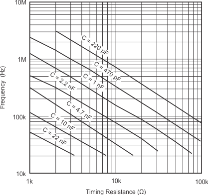
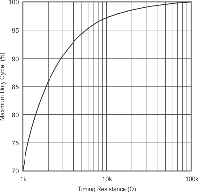
The oscillator of the UC1825A-SP is a saw tooth (see Figure 13). The rising edge is governed by a current controlled by the RT pin and value of capacitance at the CT pin (CCT). The falling edge of the sawtooth sets dead time for the outputs. Selection of RT must be done first, based on desired maximum duty cycle (see Figure 15). CT can then be chosen based on the desired frequency (RT) and DMAX (see Figure 14). Equation 2 shows the design equations.

Recommended values for RT range from 1 kΩ to 100 kΩ. Control of DMAX less than 70% is not recommended.
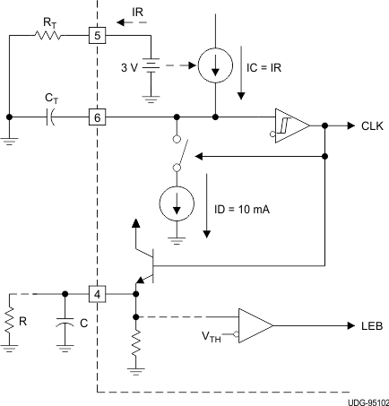 Figure 13. Oscillator
9.2 Typical Application
Power can efficiently be converted using any of several standard topologies. Design tradeoffs of cost, size and performance will generally narrow the field to one that is most appropriate.
For this application, the center-tapped push-pull configuration has been selected. Current mode control provides numerous advantages over conventional duty cycle control, and has been implemented as the regulation method.
In review, the error amplifier output (outer control loop) defines the level at which the primary current (inner loop) will regulate the pulse width, and output voltage. Pulse-by-pulse symmetry correction (flux balancing) is inherent to current mode controllers, and essential for the push-pull topology to prevent core saturation. A basic current-mode-controlled, MOSFET-switched, push-pull converter is shown in Figure 16. Transistor Q1 is turned on by a drive pulse from the PWM, causing primary current lp to flow through the transformer primary, mosfet Q1 and sense resistor Rs. Simultaneously, diode D1 conducts current Ip × Np / Ns in the secondary, storing energy in inductor L1 and delivering power to the output load. When Q1 receives a turnoff pulse from the PWM, it halts the current flow in the primary. Secondary current continues due to the filter inductor L1. Diodes D1 and D2 each conduct one-half the DC output current during these converter off times. This entire process is repeated on alternate cycles, as Q2 next is toggled on and off. The basic waveforms are shown in Figure 16 for reference.
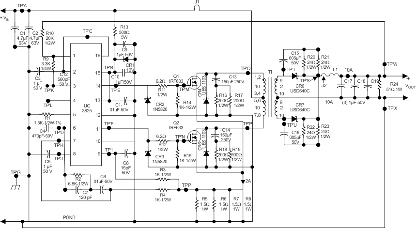 Figure 16. Typical Application Schematic
9.2.1 Design Requirements
Table 1 lists the design parameters for this example.
Table 1. Design Parameters
| DESIGN PARAMETER | EXAMPLE VALUE |
|---|---|
| Input voltage range | 42 to 56 VDC |
| Switching Frequency | 1.5 MHz |
| Output Power | 51 W Maximum |
| Output Voltage | 5.1 VDC (nom) |
| Output Current | 2-10 |
| ADC Line Regulation | 5 mV |
| Load Regulation | 15 mV |
| Output Ripple | 100 mV (typical) |
| Efficiency | 75% (typical) |
9.2.2 Detailed Design Procedure
9.2.2.1 Auxiliary Supply Voltage
The 9.2-V minimum requirement of the UC1825 and 20-V gate-source maximum of the mosfets imply an approximate range from 10 V to 18 V of inputs. The 10-V value was selected to supply both VCC and VC (totem pole outputs) while keeping power dissipation in the IC low. The circuit used is a simple resistor-Zener dissipative network with ample bypassing capacitors located near the IC to reduce noise. The oscillator frequency selected is 1.5 MHz, thus resulting in a 670-ns period.
Oscillator frequency versus Rt, Ct, and deadtime curves:
- F0 = 1.5 MHz
- T period = 670 ns
- Cl = 470 pF
- Rt = 1.5 K
Therefore;
- T (on) = 570 ns (maximum)
- T (off) = 100 ns (minimum) DUTY CYCLE
- d max = T (on) max = 570 ns = 85% T (period) 670 ns
NOTE
These times will determine the mosfet device selection and transformer turns ratio. Preliminary
9.2.2.2 Oscillator Frequency
The oscillator frequency selected is 1.5 MHz, resulting in a 670-ns period. For these equations, oscillator frequency versus Rt, Ct, and deadtime curves:
- F0 = 1.5 MHz; T period = 670 ns
- Cl = 470 pF
- Rt = 1.5 K
Therefore;
- T (on) = 570 ns (maximum)
- T (on) = 570 ns (maximum)

NOTE
These times will determine the mosfet device selection and transformer turns ratio.
9.2.2.3 Preliminary Considerations
Before designing the main transformer, several parameters must be defined and determined. Standard design procedures are used for this first-cut approximation.
9.2.2.4 Input Power

Let n = 75% for a 5 V, single output power supply.

9.2.2.5 Primary Current
The primary current can be approximated using the low-line constraints of 42-V DC as shown in Equation 6:

The primary current during the transistor on time is calculated by Equation 7:

The RMS primary current is calculated by Equation 8:

9.2.2.6 Sense Resistor R(s)
Primary current is sensed and controlled in a current mode controller by first developing a voltage proportional to the primary current, used as an input to UC1825A-SP. This is accomplished by sense resistor R(s) with a calculated value of the I limit threshold value divided by the primary current at the desired current limit point, typically 120% I (maximum) shown in Equation 9.

9.2.2.7 MOSFET DC Losses
A high-quality mosfet is used to keep both DC and switching losses low, with an R(ds) on max of 0.8 Ω (see Equation 10 to Equation 13). Calculation of the voltage drops across the device are required for the transformer design.
During an overload:
9.2.2.8 Selection of Core Material
Few manufacturers provide core loss curves for frequencies above 500 khz. To minimize power dissipation in the core, the flux density must be drastically reduced in comparison to the 20 kHz to 150 kHz versions. Typical operation is at a total flux density swing, delta B, of 0.030 Tesla (300 Gauss) while approaching the 1 MHz region. TDK’s H7C4 material was selected for it’s low loss, high frequency characteristics.
9.2.2.9 Main Transformer Design
The first step in transformer design is to determine the preliminary turns ratio. Once obtained, the minimum cross-sectional area core (Ae) can be calculated, and core selection made possible.
9.2.2.10 Calculation of Transformer
Voltages and Turns Ratio is calculated by Equation 14 through Equation 19.

The secondary is designed for excellent coupling using copper foil, and the primary has been rounded to the nearest lower turns (see Equation 20).
The actual number of both primary and secondary turns will be determined by the ferrite core characteristics as a function of operating frequency and Gauss level.
9.2.2.11 Minimum Core Size
The minimum cross-sectional area core that can be used is calculated with Equation 21 for core loss limited applications.

At first it would seem that the core area required for this 1.5-MHz switcher would be ten times smaller than that of a 150-kHz version. This would be true if the flux density, number of turns and core losses remained constant. However, losses are a function of frequency, and as frequency increases, the flux density swing (Delta B) must be drastically reduced to provide a similar core loss, hence temperature rise. In this example, an acceptable figure was selected of one percent of the total output power, or one-half watt. Empirically, this translates to a temperature rise of 25°C, at 325 Gauss (0.0325 Tesla) for cores with a cross-sectional area of 0.70 cm2, a ballpark estimate of the true core size. This formula can be rewritten as Equation 22:

Equation 22 is a more convenient formula because the right hand side of the equation contains all constants. Input voltage, frequency of operation and flux density have already been determined. The selection of core size (cross-sectional area) is inversely proportional to the number of primary turns, and conversely. Based on the five-to-one turns ratio, an original assumption of five turns for the primary would result in a large core size for this 50-W application. Alternatively, a ten turn primary is used to minimize core size.
Substituting previous values for high line operation at 0.0325 Tesla (325 Gauss) and a magnetic operating frequency of 750 kHz is calculated by Equation 23:

9.2.2.12 Core Loss Limited Conditions
As the switching frequencies are increased, generally a reduction of core size or minimum number of turns is realized. This is true, however, but only to the point at which the increasing core losses prevent a further reduction of either size or minimum turns. This crossover point occurs at different frequencies for each individual ferrite material based upon their losses and acceptable circuit losses, or temperature rise.
9.2.2.13 Core Geometry Selection
A variety of standard core shapes are available in the cross-sectional area range of 0.62 cm2 to 0.84 cm2 (see Table 2). Considerations of safety agency spacing requirements, physical dimensions, window area and relative cost of assembly must be evaluated.
Table 2. Core-Style Descriptions
| CORE STYLE | DESCRIPTION | AC (cm2) | WEIGHT (g) |
|---|---|---|---|
| PQ | PQ 20/20 | 0.62 | 15 |
| POT CORE | P 22/13 | 0.63 | 13 |
| LP | LP 22/13 | 0.68 | 21 |
| TOROID | T 28/13 | 0.76 | 26 |
| EE | EE 35/28 | 0.78 | 28 |
The LP 22/13 style was selected to easily terminate (breakout) the high current output windings. For a given cross-sectional area, it occupies less PC board space, and has good shielding characteristics.
9.2.2.14 Wire Size Selection
The single, most difficult task in high frequency magnetic design is to minimize the eddy current losses, or skin effects while optimizing wire sizes. Penetration depth refers to the thickness (or depth) into a copper conductor in which a wave will penetrate for a specific frequency. For copper at 100°C, use Equation 24:
At 750 kHz, this corresponds to 8.66 × 103 cm, or about the thickness of an AWG #39 wire. Larger size wire can be used, however the AC current flows only in the depth penetrated at the switching frequency.
For low current windings, several strands of thin wire can be paralleled, or twisted together forming a bundle. Seven wires twisted around each other closely approximate a round conductor with a net diameter of three times the individual wire diameter. This twisting is commonly done at 10-12 turns per foot, and significantly reduces parasitics between wires at high frequencies.
Medium to high current windings require the use of Litz wire, a similar bundle of numerous conductors. Copper foil is also an excellent choice.
Industry practice is to operate at 450-A (RMS) per centimeter squared, or 2.22 × 10⁻³ cm2/A, which applies to windings operating at an acceptable temperature rise (see Equation 25 through Equation 31).
9.2.2.15 Calculate Secondary RMS Current


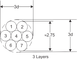 Figure 17. 7 Conductors
For a given bundle of 7 conductors as shown in Figure 17, the cross-sectional area of each conductor can be calculated by Equation 32:

The cross-sectional area of an AWG 36 wire is 1.32 × 10⁻⁴; therefore, three bundles of seven conductors each must be used. Two bundles were used as a compromise between practical winding considerations and acceptable eddy current losses.
Copper foil is used for the secondary, with a required width slightly less than the bobbin width, and thickness determined by Equation 33:

This corresponds to 0.003” thick foil, a standard value. In practice, slightly thicker foil (0.004” to 0.005”) may be required to minimize power losses in the transformer.
9.2.2.16 Transformer Assembly
Standard practice to increase coupling between primary and secondary is position both as closely as possible to each other inside the transformer. In this design, the first layer wound is one primary, and the next layer is the corresponding secondary. This is again followed by the other secondary and primary. It is important to keep the secondaries in close proximity because both will be conducting simultaneously twice per period. The primaries do not conduct in this manner, so coupling from primary A to primary B is not critical, only primary A to secondary C, and primary B to secondary D.
Referring to Figure 18, primary A is wound closest to the bobbin. After insulation, secondaries C and D are wound bifilar and insulated (see Figure 19). Primary B is wound last, then terminated so that primaries A and B are wired in series, likewise for secondaries C and D.
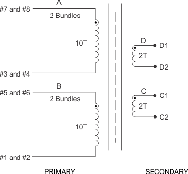 Figure 18. Transformer Schematic
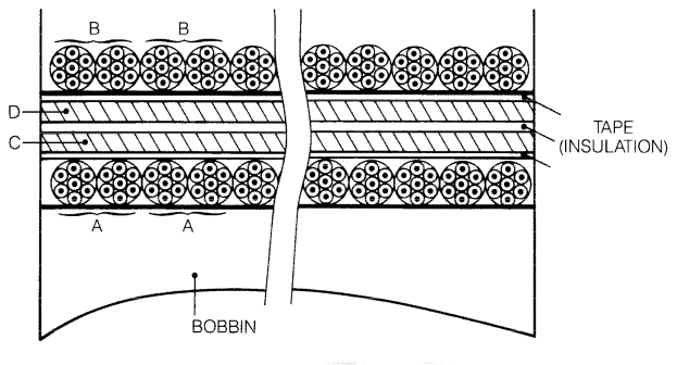 Figure 19. Transformer – Exploded View
9.2.2.17 Calculation of Winding Resistances and Losses
The mean length of turn for the bobbin can be determined from the specifications of O.D. and I.D., and for the BLP 22/13 a figure of 4.51 cm or 1.77 inches was obtained. AWG #36 wire has a resistance of 1.82 × 10⁻² Ω/cm at 100°C for the following:
Primary resistance can be calculated by Equation 34:

Voltage drop and power loss in each half winding can also be calculated by Equation 35 through Equation 37:
The resistance of the secondary can be approximated by using the wire tables, and substituting the foil for wire of similar cross-sectional area. In this example, AWG #16 wire is used to obtain Rsec = 1.58 × 10⁻⁴ Ω/cm.

9.2.2.18 Transformer Power Losses
The total copper losses for two windings are then calculated by Equation 42:
Estimated eddy current losses are approximately 50% of the copper losses. Pcu ≈ 0.50 W.
Given the core material type, geometry, frequency and operating Gauss level, the ferrite losses can be calculated. From the manufacturers information, the typical loss coefficient for H7C4 material operating at a flux density swing of 0.035 Tesla (350 Gauss) at 750 kHz is 0.15 W per cubic centimeter of core volume, which is 3.327 cm3 per LP 22/13 core set; therefore Equation 43:
The total power lost is a summation of the copper and ferrite losses calculated by Equation 44:
9.2.2.19 Output Section
9.2.2.19.1 Output Choke Calculations
Typically, the RMS output ripple current is less than 15% Idc, or 1.5 A in this case. Delta I, the peak-to-peak ripple therefore is twice the RMS, or 3 A as calculated by Equation 45.

Due to the small value of inductance required, the conventional approach will not be used. Instead, a simple RF type wound coil will be designed using the solenoid equation found in most reference texts. A thick pencil will be used as the coil form with a diameter of 0.425 inches; however, any similar item will suffice.
The form factor, F, is a function of the form diameter divided by the length of the wound coil, or D/L (see Equation 46). A few gyrations will take place before the exact values are obtained; however, this goes quickly. The form factor is listed in Table 3 for various practical values of D/L.
Table 3. Form Factor
| COIL DIAMETER, LENGTH | FORM FACTOR F |
|---|---|
| 0.1 | 0.0025 |
| 0.25 | 0.0054 |
| 0.5 | 0.01 |
| 1 | 0.0173 |
| 2 | 0.026 |
| 5 | 0.04 |
where
- D = 0.425
- D/L = 1 (approximately)
- F = 0.0173
- N = (0.690 / 0.0173 × 0.425)12 = 9.76 turns
Rounding off to the nearest next number of turns the actual inductance for 10 turns can be calculated by Equation 47:
In an air core inductor, the permeability u equals unity; therefore, the flux density B equals the driving function H.
9.2.2.19.2 Output Capacitor

where
- dV (output ripple) equals 0.1 V.
Three 1-µF capacitors are used in parallel. With a typical ripple voltage of approximately 50 mV due to ESR, the ESR each (at 1.5 mHz) must be approximately 150 mΩ. The Unitrode ceramic monolithic capacitor series was selected for their excellent high frequency characteristics.
Resonance, and its effect at these frequencies must be taken into account. In this case, the capacitor reaches resonance at 1.5 mHz, and the effective impedance is resistive.
9.2.2.19.3 Output Diodes
Schottky diodes were selected for their short reverse recovery times to minimize switching losses, and low forward drop for high DC efficiency.
9.2.2.20 UC1825A-SP PWM Control Section
9.2.2.20.1 Current Limit and Shutdown
Pulse-by-pulse current limiting is performed by the UC1825A-SP by an input of the primary current waveform to the IC at pin 9. The small RC network of R3 and C8 are used to suppress the leading edge glitch caused by turnon of the MOSFET and transformer parasitics. The input must be less than the 1-V threshold or current limiting will occur. Once reached, an input above the threshold will narrow the pulse width accordingly. When this reaches a 1.4-V amplitude, shutdown of the outputs will occur, and the UC1825A-SP will initiate a soft start routine.
9.2.2.20.2 Ramp
The UC1825A-SP offers the flexibility of both Current Mode Control or conventional duty cycle control through the RAMP input pin. When connected to the timing capacitor, the UC1825A-SP operates as a duty cycle control IC. Connecting the RAMP input to the current waveform changes the control method to Current Mode. In this application, the ramp waveform is tied through a small RC filter network to the primary current waveform. This network is defined in the next section, Slope Compensation. The dynamic range of this input is 1 V to 3 V, and is generally used for introducing slope compensation to the PWM.
9.2.2.20.3 Slope Compensation
Slope compensation is required to compensate for the peak to average differences in primary current as a function of pulse width. Adding a minimum of 50% of the reflected downslope of the output current waveform to the primary current is required. See the Unitrode application note A New Integrated Circuit for Current Mode Control (SLUA075) and the Unitrode application note Modelling, Analysis and Compensation of the Current-Mode Converter (SLUA101) for further information. Empirically, 60-75% must be used to accommodate circuit tolerances and increase stability5 Resistors R2 and R4 in this circuit form a voltage divider from the oscillator output to the RAMP input, superimposing the slope compensation on the primary current waveform. Capacitor C6 is an AC coupling capacitor, and allows the 1.8-V swing of the oscillator to be used without adding offset circuitry. Capacitor C7 has a two-fold purpose. During turnon it filters the leading edge noise of the current waveform, and provides a negative going pulse across R4 to the ramp input at the end of each cycle. This overrides any parasitic capacitance at the ramp input, (pin 7) that would tend to hold it above 0 V. This insures the proper voltage input at the beginning of the next cycle.
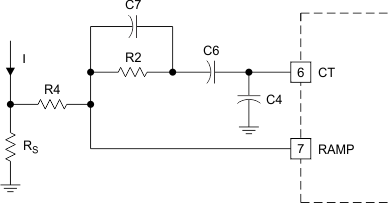 Figure 20. Slope Compensation Steps
For the purposes of determining the resistor values, capacitors C4 (timing), C6 (ac coupling) and C7 (filtering) can be removed from the circuit schematic. The simplified model represented in Figure 21 is used for the calculations in Equation 51 through Equation 61. These calculations can be applied to all current-mode circuits using a similar scheme.
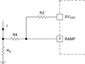 Figure 21. Slope Compensation Steps
- STEP 1. Calculate Inductor Downslope:
- STEP 2: Calculate Inductor Downslope:
- STEP 3: Calculate Equivalent Ramp Downslope Voltage:
- STEP 4: Calculate Oscillator Slope:
- STEP 5: Generate the Ramp Equations: Using superpostion, the circuit can be configured as shown in Figure 22.
- STEP 6: Calculate Slope Compensation:
- m equals the amount of inductor to be introduced.
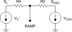 Figure 22. Slope Compensation Steps

Substituting
Where

where

Solving for R2:

Using Circuit Values:
For simplicity, let R4 equal 1 kΩ and R2 therefore equals 7.05 K. Using the nearest standard value resistor of
6.8 K, the exact amount of downslope is minimally affected. It is important that the series combination of R2 and R4 is high enough in resistance not to load down the oscillator and cause frequency shifting.
9.2.2.21 Closing the Feedback Loop
9.2.2.21.1 Error Amplifier
Compensation of the high gain error amplifier in the UC1825A-SP is straight forward. There is a single- pole at approximately 5 Hz. A zero will be introduced in the compensation network to provide gain once the zero db threshold is crossed. Using Current Mode control greatly simplifies the compensation task as the output choke is controlled by the inner current loop, thus making the output section appear as a single pole response with a zero at the ESR frequency.
9.2.2.21.2 Control to Output Gain
The control to output gain will vary with output loading, and as the load is increased the gain decreases. Output capacitor ESR will determine the frequency at which the zero occurs, thus changing the gain as a function of ESR. To ensure stability through all combinations of load and ESR, the amplifier will be compensated to cross zero db at approximately one-fifth of the switching frequency with ample phase margin.
The output filter pole and zero occur at:
Circuit Parameters:
For three capacitors in parallel:
Using the previous Equations:
Gain:

Therefore, at 2 A and 10 A:
9.2.2.21.3 Error Amplifier Compensation
The control to output gain can be plotted along with the desired zero db crossing point and an estimate of the error amplifier required compensation network can be made. The amp compensation must have a zero at approximately 100 kHz, and a gain of –16 db at this frequency. Resistor R9 has been selected to be 3.3 kΩ based on the output drive capability of the UC1825A-SP amplifier (see Specifications).
Therefore,
This compensated response can now be plotted, along with the control to output gain and the overall power supply response is a summation of the two curves, as seen in Figure 1 and Figure 2. Low-frequency gains of 100 db at full load, and 115 db at light load are obtained, with a zero db crossing at approximately 100 kHz for both. Phase margin is generous with approximately 90 degrees for both light and 45 degrees at full load. See Figure 1 and Figure 2 for more details.
Table 4. List of Materials: Capacitors
| CAPACITOR | DESCRIPTION |
|---|---|
| C1, 2 | 4.7 µF, 63 VDC Electrolytic |
| C3, 5 | 0.1 µF, 50 VDC Monolithic |
| C4 | 470 pF, VDC Monolithic |
| C6 | 0.01 µF, 50 VDC Monolithic |
| C7 | 120 pF, 50 VDC Monolithic |
| C8 | 15 pF, 50 VDC Monolithic |
| C9-11, 17-19 | 1 µF, 50 VDC Monolithic |
| C12 | 560 pF, 50 VDC Monolithic |
| C13,14 | 150 pF, 150 VDC Ceramic |
| C15, 16 | 5000 pF, 50 VDC Ceramic |
Table 5. List of Materials: Diodes
| DIODE | DESCRIPTION |
|---|---|
| CR1 | 1N4465 10 V, 1.5 W Zener |
| CR2,3 | USD1140 40 V, 1 A Schottky |
| CR4,5 | UES1105 150 V, 2.5 A Ultrafast |
| CR6,7 | USD640C 40 V, 12 ASchottky |
Table 6. List of Materials: Integrated Circuits
| INTEGRATED CIRCUIT | DESCRIPTION |
|---|---|
| U1 | UC1825A-SP TI High Speed PWM |
Table 7. List of Materials: Transistors
| TRANSISTORS | DESCRIPTION |
|---|---|
| Q1,2 | UFN633 150 V, 8A Mosfet |
Table 8. List of Materials: Resistors
| RESISTORS | DESCRIPTION |
|---|---|
| R1 | 1.5 K, 1/2 W, 1% |
| R2 | 6.8 K, 1/2 W, 5% |
| R3, 4, 14, 15 | 1 K, 1/2 W, 5% |
| R5-8 | 1.5 R, 1 W, 5% |
| R9 | 3.3 K, 1/2 W, 5% |
| R10 | 20 K, 1/2 W, 5% |
| R11, 12 | 6.2 R, 1/2 W, 5% |
| R13 | 500 R, 5W, 10% |
| R16-19 | 200 R, 1/2 W, 5% |
| R20-23 | 24 R, 1/2 W, 5% |
| R24 | 51 R, 1 W, 5% |
Table 9. List of Materials: Magnetics
| MAGNETIC | DESCRIPTION |
|---|---|
| L1 | 740 nH Wound Coil |
| T1 | AIE Magnetics Custom Transformer, 5:1 Turns Ratio |
Table 10. List of Materials: Miscellaneous
| MISCELLANEOUS | DESCRIPTION |
|---|---|
| H1 | Heatsink-Mosfets (AAALL #5786B) |
| H2 | Heatsink-Diodes (AAALL #5299B) |
Table 11. List of Materials: Efficiency Measurements
| V(IN) | I(IN) | P(IN) | P(LOSS) | EFFICIENCY |
|---|---|---|---|---|
| 42 | 1.707 | 71.1 | 20.2 | 71.8% |
| 48 | 1.483 | 71.2 | 19.7 | 72.4% |
| 56 | 1.331 | 73.2 | 21.7 | 70.4% |
Table 12. List of Materials: Efficiency Measurements
| V(IN) V | VOUT (2 A) | VOUT (5 A) | VOUT (10 A) | LOAD REGULATION (mV) |
|---|---|---|---|---|
| 42 | 5.110 | 5.102 | 5.093 | 17 |
| 48 | 5.108 | 5.101 | 5.092 | 16 |
| 56 | 5.108 | 5.102 | 5.089 | 19 |
| Line | 2 mV | 1 mV | 4 mV | — |
9.2.2.21.4 Dynamic Performance
The power supply was pulse loaded from 5 A to 10 A at a frequency of 100 kHz. Recovery to within 50 mV was less than 2 ms with a total excursion of less than 200 mV. High speed FETS were used to switch the load current with typical rise and fall times of 50 ns.
9.2.2.21.5 Short Circuit
The short circuit input current is approximately 0.75 A, or an input power of 36 W.
9.2.2.21.6 Circuit Power Losses
Table 13 lists the total circuit losses are approximated using both the calculated and measured losses throughout the power supply.
Table 13. Circuit Power-Loss Descriptions
| POWER LOSSES | VALUE |
|---|---|
| Current sense circuit | 1.2 W |
| Output Diodes | 98 W |
| Switching transistors | 3.2 W |
| Dropping resistor | 3 W |
| Snubber networks | 1 W |
| Transformer losses | 1 W |
| Auxillary supply | 0.8 W |
| Miscellaneous | 0.2 W |
| TOTAL LOSSES | 20.2 W |
If a bootstrapped technique is used in the auxiliary supply to the IC and drive circuitry, the dropping resistor losses of three watts can be reduced to 0.1 W in the bootstrap circuitry. In addition, the lossy resistive current sensing network can be replaced by a small current transformer, lowering the losses by a half-watt. Overall efficiency would then increase to 75%, fairly high for a five volt output application. Switching losses at this high of frequency can be minimized, and have little overall effect on circuit efficiency.
9.2.2.22 Summary
The demands of higher power densities will undoubtedly throttle many switch-mode power supply designs into and beyond the megahertz region in the near future. Designers will be facing the challenges of selecting switching devices, magnetic materials and IC controllers built exclusively for high efficiency at these frequencies. The thrust from contemporary hundreds of kHz designs to MHz versions is rapidly making progress. This
1.5-MHz current mode push-pull is an example of what can successfully be accomplished with existing high speed components and technology.
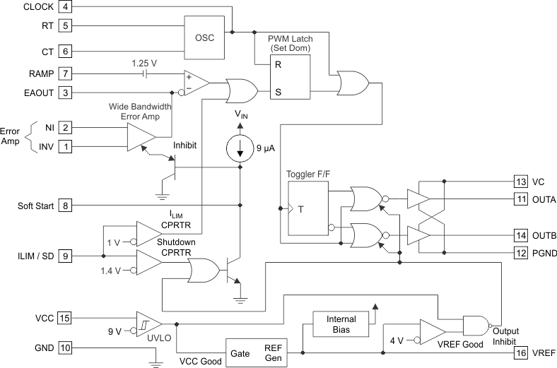 Figure 23. UC1825A-SP Block Diagram
9.2.3 Application Curves
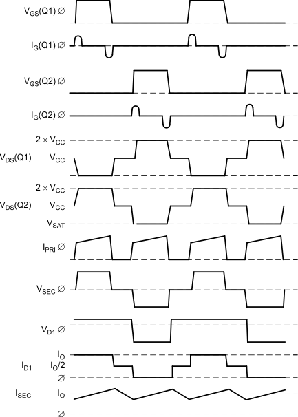 Figure 24. Basic Push-Pull Waveforms