SLUS871D January 2009 – December 2016 UC1846-SP
PRODUCTION DATA.
- 1 Features
- 2 Applications
- 3 Description
- 4 Revision History
- 5 Pin Configuration and Functions
- 6 Specifications
- 7 Detailed Description
- 8 Application and Implementation
- 9 Power Supply Recommendations
- 10Layout
- 11Device and Documentation Support
- 12Mechanical, Packaging, and Orderable Information
パッケージ・オプション
メカニカル・データ(パッケージ|ピン)
サーマルパッド・メカニカル・データ
発注情報
8 Application and Implementation
NOTE
Information in the following applications sections is not part of the TI component specification, and TI does not warrant its accuracy or completeness. TI’s customers are responsible for determining suitability of components for their purposes. Customers should validate and test their design implementation to confirm system functionality.
8.1 Application Information
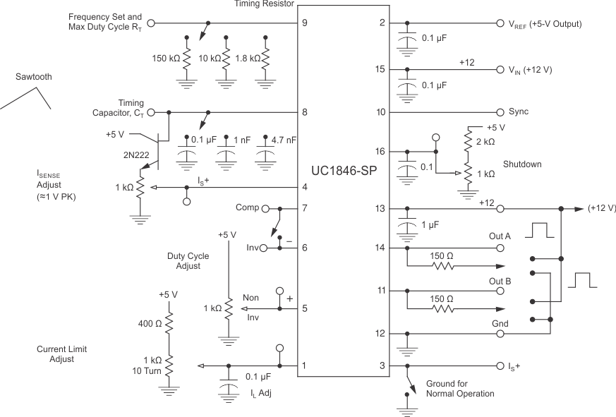
UC1846-SP can be used as a controller to design various topologies such as push-pull, half-bridge, full bridge, and flyback.
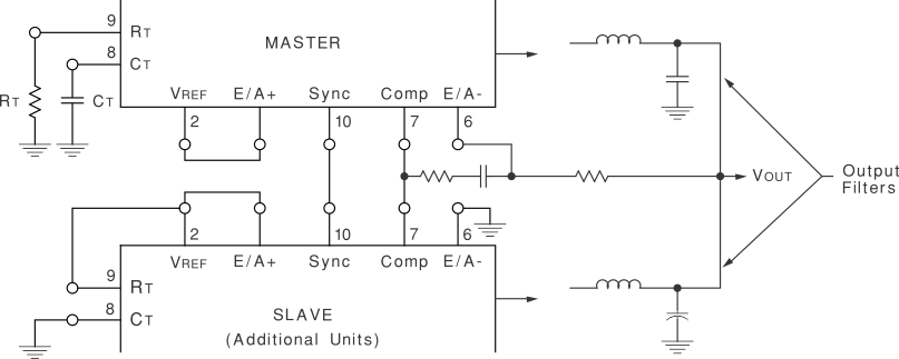
The following sections highlight the topologies for oscillators, error amplifiers, and parallel configurations (paralleling two EVMs).
8.2 Typical Applications
8.2.1 Oscillator Circuit Application

8.2.1.1 Design Requirements
8.2.1.2 Detailed Design Procedure
8.2.1.2.1 Input Capacitor Selection
Load current, duty cycle, and switching frequency are several factors which determine the magnitude of the input ripple voltage. Without the input capacitor, the pulsating current of Q1 would need to be completely supplied by the host source, VIN, which commonly does not have sufficiently low output impedance. Thus there would be substantial noise on the host DC voltage source and an increase in the conducted EMI on the board. The input capacitor, CIN, effectively filters the input current so the current from the host DC source is approximately an average current.
The input ripple voltage amplitude is directly proportional to the output load current. The maximum input ripple amplitude occurs at maximum output load. Also, the amplitude of the voltage ripple varies with the duty cycle of the converter.
UC1846-SP requires a high quality ceramic, type X5R or X7R, input decoupling capacitor of at least 47 μF of effective capacitance on the VIN input voltage pins. In some applications additional bulk capacitance may also be required for the VIN input. The effective capacitance includes any DC bias effects. The voltage rating of the input capacitor must be greater than the maximum input voltage. The capacitor must also have a ripple current rating greater than the maximum input current ripple of the UC1846-SP. The input ripple current can be calculated using Equation 4.

The value of a ceramic capacitor varies significantly over temperature and the amount of DC bias applied to the capacitor. The capacitance variations due to temperature can be minimized by selecting a dielectric material that is stable over temperature. X5R and X7R ceramic dielectrics are usually selected for power regulator capacitors because they have a high capacitance to volume ratio and are fairly stable over temperature. The output capacitor must also be selected with the DC bias taken into account. The capacitance value of a capacitor decreases as the DC bias across a capacitor increases.
The input capacitance value determines the input ripple voltage of the regulator. The input voltage ripple can be calculated using Equation 5.

8.2.1.2.2 Output Capacitor Selection
The output capacitance of a switching regulator is a vital part of the overall feedback system. The energy storage inductor and the output capacitor form a second-order low-pass filter.
In switching power supply power stages, the function of output capacitance is to store energy. The energy is stored in the capacitor’s electric field due to the voltage applied. Thus, qualitatively, the function of a capacitor is to attempt to maintain a constant voltage.
The value of output capacitance of a buck power stage is generally selected to limit output voltage ripple to the level required by the specification. Since the ripple current in the output inductor is usually already determined, the series impedance of the capacitor primarily determines the output voltage ripple. The three elements of the capacitor that contribute to its impedance (and output voltage ripple) are equivalent series resistance (ESR), equivalent series inductance (ESL), and capacitance (C). The following gives guidelines for output capacitor selection.
For continuous inductor current mode operation, to determine the amount of capacitance needed as a function of inductor current ripple, ΔIL, switching frequency, fS, and desired output voltage ripple, ΔVO, Equation 6 is used assuming all the output voltage ripple is due to the capacitor’s capacitance.

where
Each capacitor type is characterized by its impedance and the frequency range over which it is most effective. The frequency at which the impedance reaches its minimum is determined by its ESR and ESL. It is known as the self resonant frequency of the capacitor. The self resonant frequency is considered to be the maximum usable frequency for a capacitor. Above this frequency the impedance of the capacitor begins to rise as the ESL of the capacitor begins to dominate. Note that each capacitor type has a specific frequency band over which it is most effective. Therefore, a capacitor network of multiple capacitor types is more effective in reducing impedance than just one type.
The current slew rate of a regulator is limited by its output filter inductor. When the amount of current required by the load changes, the initial current deficit must be supplied by the output capacitors until the regulator can meet the load demand.
The desired response to a large change in the load current is the first criteria. The output capacitor needs to supply the load with current when the regulator control loop can not supply the current. This happens when Load (ie: memory, processor) has a large and fast increase in current, such as a transition from no load to full load. The regulator typically needs two or more clock cycles for the control loop to see the change in load current, output voltage and adjust the duty cycle to react to the change. The output capacitor must be properly sized to supply the extra current to the Load until the control loop responds to the Load change. The output capacitance must be large enough to supply the difference in current for 2 clock cycles while only allowing a tolerable amount of droop in the output voltage. Equation 7 shows the minimum output capacitance necessary to accomplish this.

Where ΔIout is the change in output current, fSW is the regulators switching frequency and ΔVout is the allowable change in the output voltage. For this example, the transient load response is specified as a 5% change in Vout for a load step of 1 A. For this example, ΔIout = 1 A and ΔVout = 0.05 × 3.3 = 0.165 V. Using these numbers gives a minimum capacitance of 25 μF. This value does not take the ESR of the output capacitor into account in the output voltage change. For ceramic capacitors, the ESR is usually small enough to ignore in this calculation.
8.2.1.2.3 Output Inductor Selection
To calculate the value of the output inductor, use Equation 8. Kind is a coefficient that represents the amount of inductor ripple current relative to the maximum output current. The inductor ripple current is filtered by the output capacitor. Therefore, choosing high inductor ripple currents impact the selection of the output capacitor since the output capacitor must have a ripple current rating equal to or greater than the inductor ripple current. In general, the inductor ripple value is at the discretion of the designer; however, Kind is normally from 0.1 to 0.3 for the majority of applications. VinLC refers to the voltage at the input of output LC filter.

The current flowing through the inductor is the inductor ripple current plus the output current. During power up, faults or transient load conditions, the inductor current can increase above the calculated peak inductor current level calculated above. In transient conditions, the inductor current can increase up to the switch current limit of the device. For this reason, the most conservative approach is to specify an inductor with a saturation current rating equal to or greater than the switch current limit rather than the peak inductor current.
8.2.1.2.4 Switching Frequency
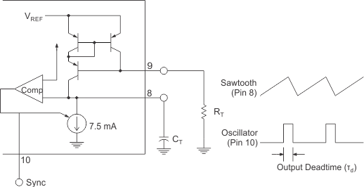
Initial accuracy of UC1846-SP oscillator frequency is 200 kHz ±15% over the temperature range. Switching frequency selection is a trade-off between the overall design size and efficiency. Operating at lower switching frequency will result in higher efficiency at the expense of larger solution footprint.
Oscillator frequency can be determined as follows:

8.2.1.3 Application Curves
| VIN = 20 V | TJ = 25°C | |
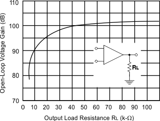
| VIN = 20 V | TJ = 25°C | |
8.2.2 Parallel Operation
8.2.2.1 Design Requirements
Refer to Design Requirements for the oscillator circuit design requirements.
8.2.2.2 Detailed Design Procedure
Refer to Detailed Design Procedure for the oscillator circuit detailed design procedure.
8.2.3 Soft-Start and Shutdown/Restart Functions Application
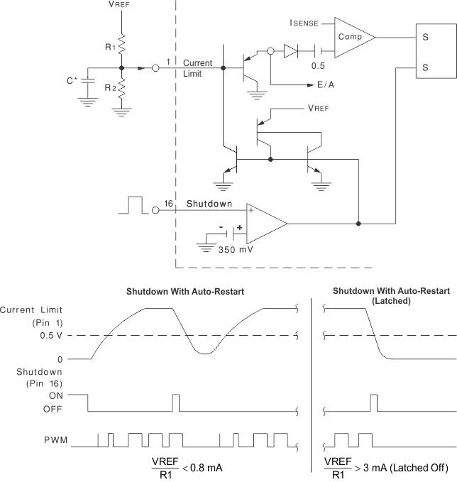
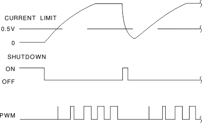
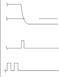
 , the shutdown latch commutates when ISS = 0.8 mA and a restart cycle will be initiated.
 , the device latches off until power is recycled.
8.2.4 Open-Loop Test Circuit Application
