SLUS871D January 2009 – December 2016 UC1846-SP
PRODUCTION DATA.
- 1 Features
- 2 Applications
- 3 Description
- 4 Revision History
- 5 Pin Configuration and Functions
- 6 Specifications
- 7 Detailed Description
- 8 Application and Implementation
- 9 Power Supply Recommendations
- 10Layout
- 11Device and Documentation Support
- 12Mechanical, Packaging, and Orderable Information
パッケージ・オプション
メカニカル・データ(パッケージ|ピン)
サーマルパッド・メカニカル・データ
発注情報
5 Pin Configuration and Functions
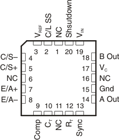
FK Package
20-Pin LCCC
Top View

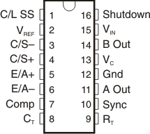
J or W Package
16-Pin CDIP or CFP
Top View

Pin Functions
| PIN | I/O | DESCRIPTION | ||
|---|---|---|---|---|
| NAME | CDIP or CFP | LCCC | ||
| CL SS | 1 | 2 | I | Current limit/soft-start. |
| VREF | 2 | 3 | O | 5.1-V internally generated reference. |
| CS- | 3 | 4 | I | Inverting input of current sense operational amplifier. |
| CS+ | 4 | 5 | I | Non-Inverting input of current sense operational amplifier. |
| EA+ | 5 | 7 | I | Non-Inverting input of error amplifier. |
| EA- | 6 | 8 | I | Inverting input of error amplifier. |
| COMP | 7 | 9 | O | Output of error amplifier. |
| CT | 8 | 10 | I | Timing capacitance. Capacitor connected from CT to ground is charged via current established by RT pin via current mirror. Output pulse dead time is determined by the size of the capacitor during capacitor discharge time. |
| RT | 9 | 12 | I | Determines oscillator frequency. VREF sources thru RT to create a current which is mirrored to CT pin. |
| SYNC | 10 | 13 | I/O | Sync pin is an output under normal operation when RT is above 4.1-V sync output high. Sync pin is an input when RT pin is high and CT pin tied low. |
| AOUT | 11 | 14 | O | Output driver (source/sink). |
| GND | 12 | 15 | — | Ground connection. |
| VC | 13 | 17 | I | Gate drive collector supply voltage. Decouple with capacitor. |
| BOUT | 14 | 18 | O | Output driver (source/sink). |
| VIN | 15 | 19 | I | Input voltage decouple with capacitor. |
| SHUTDOWN | 16 | 20 | I | Shutdown threshold 350 mV. Voltage above threshold latches off oscillator. |
| NC | — | 1, 6, 11 | — | No connect. |
Bare Die Information
| DIE THICKNESS | BACKSIDE FINISH | BACKSIDE POTENTIAL | BOND PAD METALLIZATION COMPOSITION | BOND PAD THICKNESS |
|---|---|---|---|---|
| 15 mils | Silicon with backgrind | Floating | AlCu2% | 2000 nm |

Bond Pad Coordinates in Microns
| DESCRIPTION | PAD NUMBER | X MIN | Y MIN | X MAX | Y MAX |
|---|---|---|---|---|---|
| Current limit/soft-start | 1 | 2174.24 | 1661.16 | 2280.92 | 1767.84 |
| VREF | 2 | 2235.2 | 2026.92 | 2341.88 | 2133.6 |
| (–) Current sense | 3 | 1996.44 | 2219.96 | 2103.12 | 2326.64 |
| (+) Current sense | 4 | 1635.76 | 2219.96 | 1742.44 | 2326.64 |
| (+) Error amplifier | 5 | 467.36 | 2219.96 | 574.04 | 2326.64 |
| (–) Error amplifier | 6 | 289.56 | 2219.96 | 396.24 | 2326.64 |
| Compensation | 7 | 142.24 | 1671.32 | 248.92 | 1778 |
| CT | 8 | 157.48 | 1270 | 264.16 | 1376.68 |
| RT | 9 | 157.48 | 939.8 | 264.16 | 1046.48 |
| SYNC | 10 | 157.48 | 172.72 | 264.16 | 279.4 |
| OUTPUT A | 11 | 772.16 | 213.36 | 889 | 350.52 |
| GROUND | 12 | 1346.2 | 81.28 | 1463.04 | 208.28 |
| VC | 13 | 1341.12 | 472.44 | 1468.12 | 645.16 |
| OUTPUT B | 14 | 1920.24 | 213.36 | 2037.08 | 350.52 |
| VIN | 15 | 2255.52 | 320.04 | 2362.2 | 426.72 |
| SHUTDOWN | 16 | 2214.88 | 1107.44 | 2321.56 | 1214.12 |