SLUS352C January 1997 – December 2015 UC1846 , UC2846 , UC3846 , UC3847
PRODUCTION DATA.
- 1 Features
- 2 Applications
- 3 Description
- 4 Revision History
- 5 Pin Configuration and Functions
- 6 Specifications
- 7 Detailed Description
- 8 Application and Implementation
- 9 Power Supply Recommendations
- 10Layout
- 11Device and Documentation Support
- 12Mechanical, Packaging, and Orderable Information
パッケージ・オプション
デバイスごとのパッケージ図は、PDF版データシートをご参照ください。
メカニカル・データ(パッケージ|ピン)
- J|16
- FK|20
サーマルパッド・メカニカル・データ
発注情報
7 Detailed Description
7.1 Overview
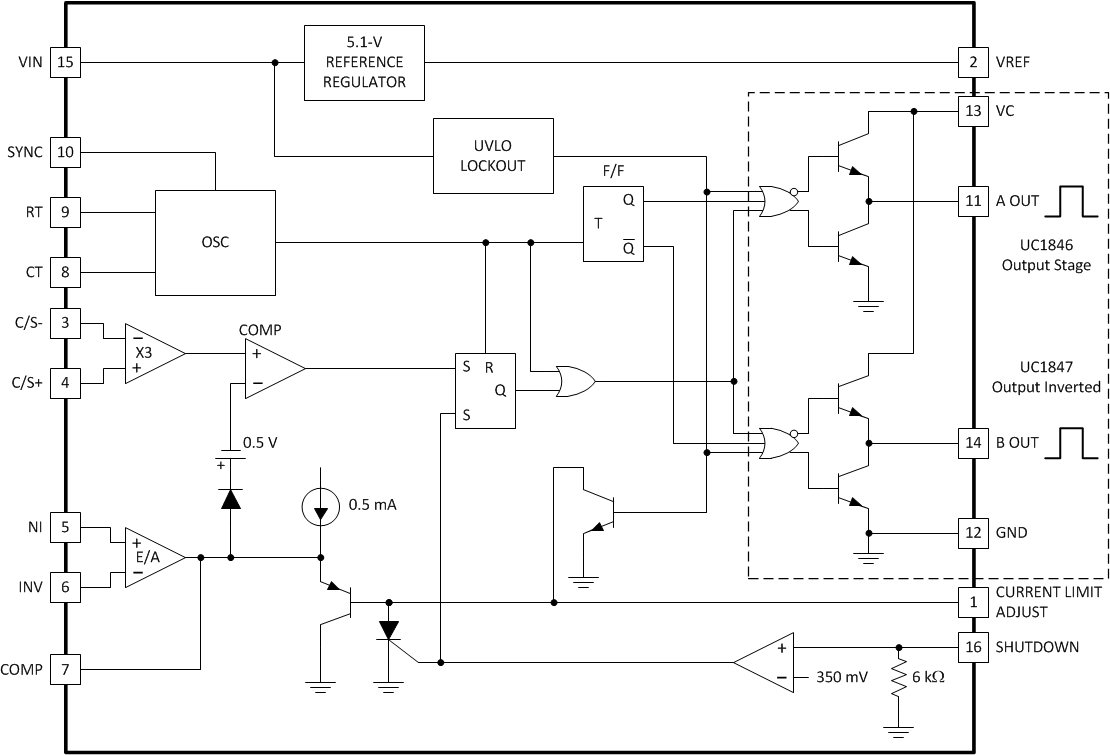
The UCx846/7 family of control devices provides the necessary features to implement off-line or DC-to-DC fixed-frequency, current-mode control schemes with a minimal external parts count. Internally implemented circuits include under-voltage lockout featuring start-up current less than 1 mA, a precision reference trimmed for accuracy at the error amplifier input, logic to insure latched operation, a PWM comparator which also provides current limit control, and a totem pole output stage designed to source or sink high-peak current. The output stage, suitable for driving either N-Channel MOSFETs or bipolar transistor switches, is low in the off state.
7.2 Functional Block Diagram

7.3 Feature Description
7.3.1 Current Sense Amplifier
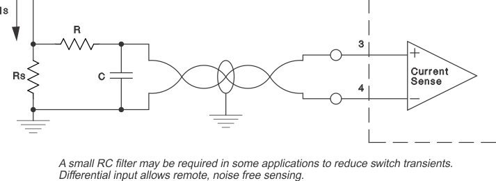
The current sense amplifier may be used in a variety of ways to sense peak switch current for comparison with an error voltage. Referring to Functional Block Diagram, maximum swing on the inverting input of the PWM comparator is limited to approximately 3.5 V by the internal regulated supply. Accordingly, for a fixed gain of 3, maximum differential voltages must be kept below 1.2 V at the current sense inputs.
 Figure 3. Current Sense Amplifier Connection
7.3.2 Oscillator
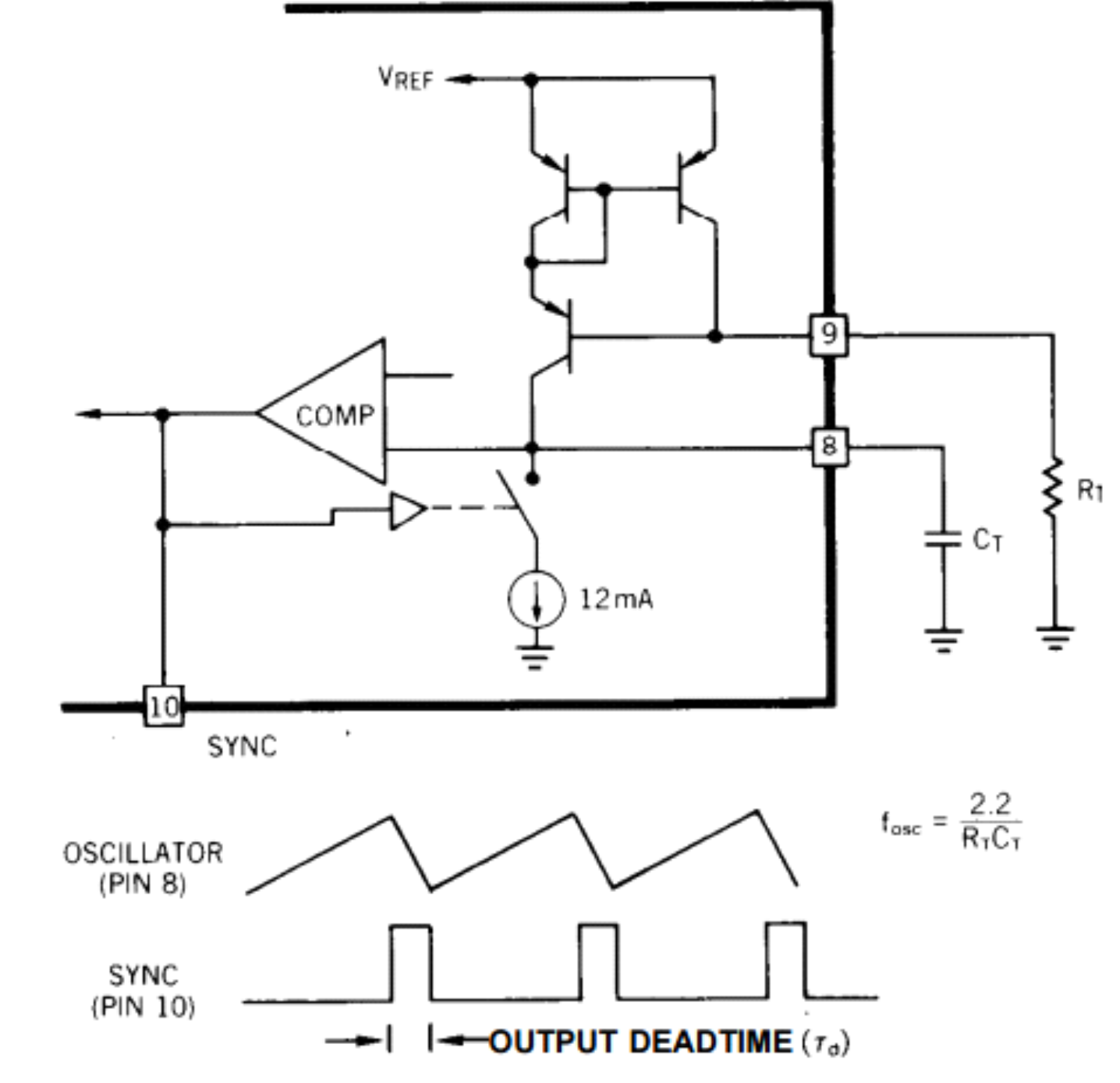
By implementing the oscillator using all NPN transistors, the UCx846/7 achieves excellent temperature stability and waveform clarity at frequencies in excess of 1 MHz.
Referring to Figure 4, an external resistor RT is used to generate a constant current into a capacitor CT to produce a linear sawtooth waveform. Oscillator frequency may be approximated by selecting RT and CT such that:

 Figure 4. Oscillator Circuit
7.4 Device Functional Modes
7.4.1 Current Limit
One of the most attractive features of a current-mode converter is the ability to limit peak-switch currents on a pulse-by-pulse basis by simply limiting the error voltage to a maximum value.
7.4.2 Shutdown
The shutdown circuit was designed to provide a fast acting general purpose shutdown port for use in implementing both protection circuitry and remote shutdown functions. The circuit may be divided into an input section consisting of a comparator with a 350-mV temperature compensated offset, and an output section consisting of a three transistor latch. Shutdown is accomplished by applying a signal greater than 350 mV to pin 16, causing the output latch to fire, and setting the PWM latch to provide an immediate signal to the outputs.