SLUS191D February 1997 – July 2017 UC1525A , UC1527A , UC2525A , UC2527A , UC3525A , UC3527A
PRODUCTION DATA.
- 1 Features
- 2 Applications
- 3 Description
- 4 Revision History
- 5 Pin Configuration and Functions
- 6 Specifications
- 7 Detailed Description
- 8 Application and Implementation
- 9 Power Supply Recommendations
- 10Layout
- 11Device and Documentation Support
- 12Mechanical, Packaging, and Orderable Information
パッケージ・オプション
デバイスごとのパッケージ図は、PDF版データシートをご参照ください。
メカニカル・データ(パッケージ|ピン)
- DW|16
- N|16
サーマルパッド・メカニカル・データ
発注情報
5 Pin Configuration and Functions
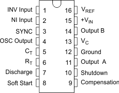
J and N Package
16-Pin CDIP and PDIP
Top View

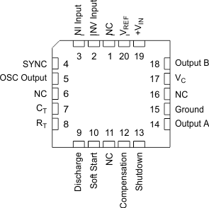
FN and FK Packages
20-Pin PLCC or LCCC
Top View

Pin Functions
| PIN | I/O | DESCRIPTION | ||
|---|---|---|---|---|
| NAME | CDIP, PDIP |
PLCC, LCCC |
||
| INV Input | 1 | 2 | I | Inverting input to the error amplifier |
| NI Input | 2 | 3 | I | Noninverting input to the error amplifier |
| SYNC | 3 | 4 | I | Oscillator sync terminal |
| OSC Output | 4 | 5 | O | Oscillator frequency output |
| CT | 5 | 7 | I | Timing capacitor connection pin for oscillator frequency programming. The timing capacitor should be connected to the device ground using minimal trace length. |
| RT | 6 | 8 | I | Timing resistor connection pin for oscillator frequency programming |
| Discharge | 7 | 9 | I | A single resistor between CT and the discharge terminals provides dead-time adjustment |
| Soft Start | 8 | 10 | I | Soft-start input pin. |
| Compensation | 9 | 12 | O | Output of the error amplifier for compensation |
| Shutdown | 10 | 13 | I | Pull this pin high to shut down PWM output |
| Output A | 11 | 14 | O | output A of the on-chip drive stage |
| Ground | 12 | 15 | — | Ground return pin |
| VC | 13 | 17 | — | Power supply pin for the output stage. This pin should be bypassed with a 0.1-µF monolithic ceramic low ESL capacitor with minimal trace lengths. |
| Output B | 14 | 18 | O | Output B of the on-chip drive stage. |
| +VIN | 15 | 19 | — | Input voltage |
| VREF | 16 | 20 | O | 5.1-V reference. For stability, the reference should be bypassed with a 0.1-µF monolithic ceramic low ESL capacitor and minimal trace length to the ground plane. |
| NC | — | 1, 6, 11, 16 | — | No internal connection |