SLUS557G March 2003 – December 2016 UC28023 , UC28025
PRODUCTION DATA.
- 1 Features
- 2 Applications
- 3 Description
- 4 Revision History
- 5 Pin Configuration and Functions
- 6 Specifications
- 7 Parameter Measurement Information
- 8 Detailed Description
- 9 Application and Implementation
- 10Power Supply Recommendations
- 11Layout
- 12Device and Documentation Support
- 13Mechanical, Packaging, and Orderable Information
パッケージ・オプション
デバイスごとのパッケージ図は、PDF版データシートをご参照ください。
メカニカル・データ(パッケージ|ピン)
- N|16
- DW|16
サーマルパッド・メカニカル・データ
発注情報
6 Specifications
6.1 Absolute Maximum Ratings
over operating free-air temperature range (unless otherwise noted)(1)(2)| MIN | MAX | UNIT | |||
|---|---|---|---|---|---|
| Input voltage | VC, VCC | 30 | V | ||
| Analog inputs | INV, NI, RAMP | –0.3 | 7 | V | |
| SS, ILIM/SD | VREF – 0.3 | VREF + 0.3 | |||
| IOUT(DC) | Output current | OUT (UC28023), OUTB (UC28025) | ±0.5 | A | |
| Peak output current, pulsed 0.5 ms (IOUT pulsed) | OUT (UC28023), OUTB (UC28025) | ±2 | A | ||
| IREF | Output current | VREF | 10 | mA | |
| ICLOCK | Output current | CLOCK | –5 | mA | |
| ISINK_SS | Soft-start sink current | SS | 5 | mA | |
| IOUT(EA) | Output current | EAOUT | 20 | mA | |
| IOSC_CHG | Oscillator charging current | RT | –5 | mA | |
| CLOAD | Capacitive load | 200 | pF | ||
| Power Dissipation at TA = 25°C (all packages) | 1 | W | |||
| TJ | Operating junction temperature | –55 | 150 | °C | |
| Tstg | Storage temperature | –65 | 150 | °C | |
(1) Stresses beyond those listed under Absolute Maximum Ratings may cause permanent damage to the device. These are stress ratings only, which do not imply functional operation of the device at these or any other conditions beyond those indicated under Recommended Operating Conditions. Exposure to absolute-maximum-rated conditions for extended periods may affect device reliability.
(2) All voltages are with respect to GND. All currents are positive into and negative out of the specified terminal.
6.2 ESD Ratings
| VALUE | UNIT | |||
|---|---|---|---|---|
| V(ESD) | Electrostatic discharge | Human-body model (HBM), per ANSI/ESDA/JEDEC JS-001(1) | ±3000 | V |
| Charged-device model (CDM), per JEDEC specification JESD22-C101(2) | ±1500 | |||
(1) JEDEC document JEP155 states that 500-V HBM allows safe manufacturing with a standard ESD control process.
(2) JEDEC document JEP157 states that 250-V CDM allows safe manufacturing with a standard ESD control process.
6.3 Recommended Operating Conditions
over operating free-air temperature range (unless otherwise noted)| MIN | NOM | MAX | UNIT | |
|---|---|---|---|---|
| VCC input voltage from a low-impedance source | 12 | V | ||
| Operating temperature | –40 | 105 | °C |
6.4 Thermal Information
| THERMAL METRIC(1) | UC2802x | UNIT | ||
|---|---|---|---|---|
| DW (SOIC) | N (PDIP) | |||
| 16 PINS | 16 PINS | |||
| RθJA | Junction-to-ambient thermal resistance | 70.5 | 44.5 | °C/W |
| RθJC(top) | Junction-to-case (top) thermal resistance | 31.8 | 34.3 | °C/W |
| RθJB | Junction-to-board thermal resistance | 35.2 | 24.6 | °C/W |
| ψJT | Junction-to-top characterization parameter | 7.7 | 14.7 | °C/W |
| ψJB | Junction-to-board characterization parameter | 34.7 | 24.4 | °C/W |
(1) For more information about traditional and new thermal metrics, see the Semiconductor and IC Package Thermal Metrics application report.
6.5 Electrical Characteristics
TA = –40°C to 105°C, TJ = TA, RT = 3.65 kΩ, CT = 1 nF, VCC = 15 V (unless otherwise noted)| PARAMETER | TEST CONDITIONS | MIN | TYP | MAX | UNIT | ||
|---|---|---|---|---|---|---|---|
| REFERENCE | |||||||
| VREF | Reference voltage | TJ = 25°C, IREF = 1 mA | 5.05 | 5.1 | 5.15 | V | |
| Line regulation voltage | VCC = 10 V to 30 V | 2 | 15 | mV | |||
| Load regulation voltage | IREF = 1 mA to 10 mA | 5 | 15 | mV | |||
| Temperature stability(1) | TA = –40°C to 105°C | 0.2 | 0.4 | mV/°C | |||
| Total output voltage variation(1) | Line and load temperature | 4.95 | 5.25 | V | |||
| Output noise voltage(1) | f = 10 Hz to 10 kHz | 50 | µV | ||||
| Long-term stability voltage(1) | TJ = 125°C, 1000 hours | 5 | 25 | mV | |||
| ISS | Short-circuit current | VREF = 0 V | –20 | –50 | –100 | mA | |
| OSCILLATOR | |||||||
| fOSC | Initial accuracy(1) | TJ = 25°C | 360 | 400 | 440 | kHz | |
| Voltage stability(1) | VCC =10 V to 30 V | 0.2% | 2% | ||||
| Temperature stability(1) | TA = –40°C to 105°C | 5% | |||||
| Total voltage variation(1) | Line temperature | 340 | 460 | kHz | |||
| VCLOCK_H | High-level clock output voltage | 3.9 | 4.5 | V | |||
| VCLOCK_L | Low-level clock output voltage | 2.3 | 2.9 | V | |||
| VRAMP(P) | Ramp peak voltage(1) | 2.6 | 2.8 | 3 | V | ||
| VRAMP(V) | Ramp valley voltage(1) | 0.7 | 1 | 1.25 | V | ||
| VRAMP(VP) | Ramp valley-to-peak voltage(1) | 1.6 | 1.8 | 2 | V | ||
| ERROR AMPLIFIER | |||||||
| VIN | Input offset voltage | 15 | mV | ||||
| IBIAS | Input bias current | 0.6 | 3 | µA | |||
| IIN | Input offset current | 0.1 | 1 | µA | |||
| AVOL | Open-loop gain | VOUT = 1 V to 4 V | 60 | 95 | dB | ||
| CMRR | Common-mode rejection ratio | VCM = 1.5 V to 5.5 V | 75 | 95 | dB | ||
| PSRR | Power supply rejection ratio | VCC = 10 V to 30 V | 85 | 110 | dB | ||
| IOUT(SINK) | Output sink current | V(EAOUT) = 1 V | 1 | 2.5 | mA | ||
| IOUT(SRC) | Output source current | V(EAOUT) = 4 V | –0.5 | –1.3 | mA | ||
| VOH | High-level output voltage | I(EAOUT) = –0.5 V | 4 | 4.7 | 5 | V | |
| VOL | Low-level output voltage | I(EAOUT) = 1 mA | 0 | 0.5 | 1 | V | |
| Unity gain bandwidth(1) | 3 | 5.5 | MHz | ||||
| Slew rate(1) | 6 | 12 | V/µs | ||||
| PWM COMPARATOR | |||||||
| IBIAS_RAMP | RAMP bias current | VRAMP = 0 V | –1 | –5 | µA | ||
| Maximum duty cycle | UC28023 | 80% | 90% | ||||
| UC28025 | See (2) | 40% | 45% | ||||
| Minimum duty cycle | UC28023 | 0% | |||||
| UC28025 | 0% | ||||||
| EAOUT zero DC threshold | VRAMP = 0 V | 1.1 | 1.25 | 1.4 | V | ||
| SOFT START | |||||||
| ICHG | Charge current | VSS = 0.5 V | 3 | 9 | 20 | µA | |
| IDISCHG | Discharge current | VSS = 1 V | 1 | 7.5 | mA | ||
| CURRENT LIMIT AND SHUTDOWN | |||||||
| ILIMIT | Current limit bias current | VILIM/SD = 0 V to 4 V | ±10 | µA | |||
| ILIMIT | Offset voltage | UC28023 | 15 | mV | |||
| ILIMITREF | Common mode(1) | UC28023 | 1 | 1.25 | V | ||
| Current limit threshold voltage | UC28025 | 0.9 | 1 | 1.1 | V | ||
| Shutdown threshold voltage | 1.25 | 1.4 | 1.55 | V | |||
| OUTPUT | |||||||
| VOL | Low-level output voltage | IOUT = 20 mA | 0.25 | 0.4 | V | ||
| IOUT = 200 mA | 1.2 | 2.2 | |||||
| VOH | High-level output voltage | IOUT = –20 mA | 13 | 13.5 | V | ||
| IOUT = –200 mA | 12 | 13 | |||||
| Collector leakage | VC = 30 V | 100 | 500 | µA | |||
| UNDERVOLTAGE LOCKOUT (UVLO) | |||||||
| Start threshold voltage | 8.8 | 9.2 | 9.6 | V | |||
| Hysteresis | 0.4 | 0.8 | 1.2 | V | |||
| SUPPLY CURRENT | |||||||
| Start-up current | VCC = 8 V | 1.1 | 2 | mA | |||
| ICC | Operating current | VINV = VRAMP = VILIM = 0 V, VNI = 1 V |
25 | 35 | mA | ||
(1) Specified by design. Not production tested.
(2) Tested as 80% minimum for the oscillator which is the equivalent of 40% for UC28025.
6.6 Switching Characteristics
over operating free-air temperature range (unless otherwise noted)| PARAMETER | TEST CONDITIONS | MIN | TYP | MAX | UNIT | ||
|---|---|---|---|---|---|---|---|
| tDELAY | Delay to output time(1) | PWM comparator | 50 | 100 | ns | ||
| Current limit and shutdown | 50 | 80 | ns | ||||
| Rise time and Fall time(1) | CLOAD = 1 nF | 30 | 60 | ns | |||
6.7 Typical Characteristics
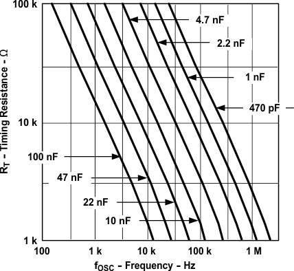 Figure 1. Timing Resistance vs Frequency
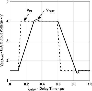 Figure 3. Unity Gain Slew Rate
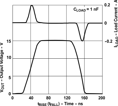 Figure 5. Rise and Fall Time vs
Output Voltage and Load Current
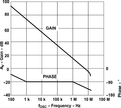 Figure 2. Open-Loop Frequency Response
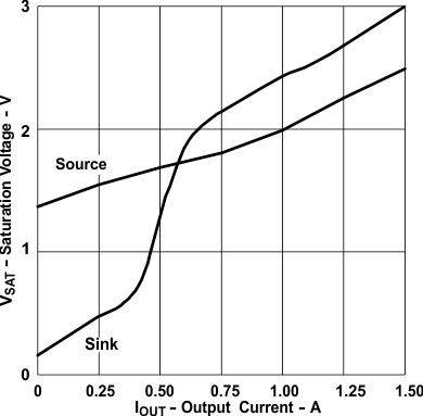 Figure 4. Saturation Voltage vs Output Current
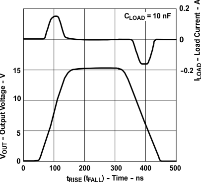 Figure 6. Rise and Fall Time vs
Output Voltage and Load Current