SLUS352C January 1997 – December 2015 UC1846 , UC2846 , UC3846 , UC3847
PRODUCTION DATA.
- 1 Features
- 2 Applications
- 3 Description
- 4 Revision History
- 5 Pin Configuration and Functions
- 6 Specifications
- 7 Detailed Description
- 8 Application and Implementation
- 9 Power Supply Recommendations
- 10Layout
- 11Device and Documentation Support
- 12Mechanical, Packaging, and Orderable Information
パッケージ・オプション
デバイスごとのパッケージ図は、PDF版データシートをご参照ください。
メカニカル・データ(パッケージ|ピン)
- N|16
- DW|16
サーマルパッド・メカニカル・データ
発注情報
8 Application and Implementation
NOTE
Information in the following applications sections is not part of the TI component specification, and TI does not warrant its accuracy or completeness. TI’s customers are responsible for determining suitability of components for their purposes. Customers should validate and test their design implementation to confirm system functionality.
8.1 Application Information
The UCx846/7 family of control devices provides all of the necessary features to implement fixed frequency, current mode control schemes while maintaining a minimum external parts count. The superior performance of this technique can be measured in improved line regulation, enhanced load response characteristics, and a simpler, easier to design control loop. Topological advantages include inherent pulse-by-pulse current limiting capability, automatic symmetry correction for push-pull converters. Protection circuitry includes undervoltage lockout and programmable current limit in addition to soft-start capability. A shutdown function is also available which initiates either a complete shutdown with automatic restart or latch the supply off.
8.2 Typical Application
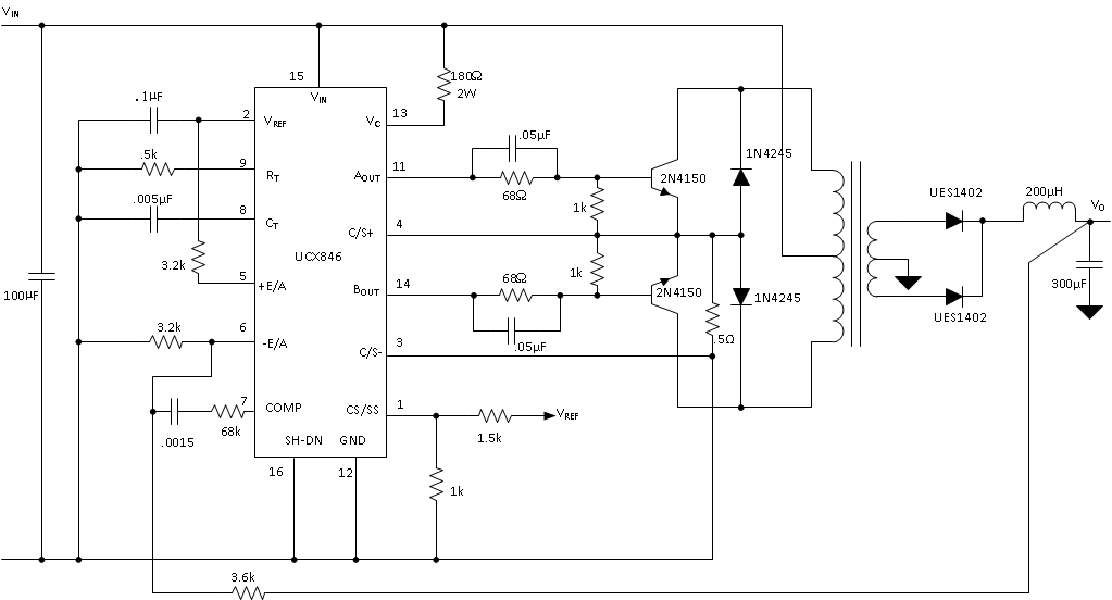 Figure 5. Typical Application Diagram
8.2.1 Design Requirements
Table 1 shows the design parameters for this application.
Table 1. Design Parameters
| DESIGN PARAMETER | TARGET VALUE |
|---|---|
| Typical efficiency | 85% |
| Switching frequency | 880 kHz |
| Pulse by pulse current limit threshold | 1 A |
8.2.2 Detailed Design Procedure
This section details the design procedure based on the design requirements.
8.2.2.1 Design Switching Frequency
Output deadtime is determined by the external capacitor, CT, according to the formula:

where
- ID = Oscillator discharge current at 25°C; typically is 7.5.
For large values of RT: τd (μs ) ≈145CT (μF).
Oscillator frequency is approximated by the formula:

8.2.2.2 Error Amplifier Output Configuration
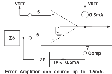 Figure 6. Error Amplifier Output Configuration
8.2.2.3 Parallel Operation Configuration
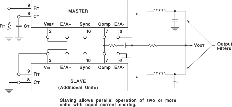 Figure 7. Parallel Operation
8.2.2.4 Design Pulse by Pulse Current Limit Threshold
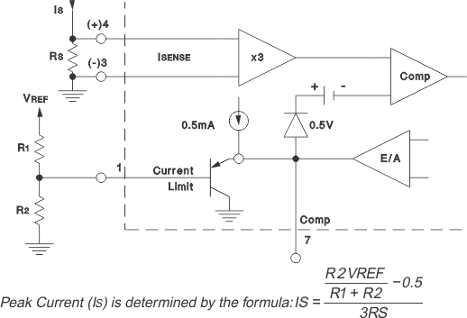 Figure 8. Pulse by Pulse Current Limiting
8.2.2.5 Soft-Start and Shutdown, Restart Function Design
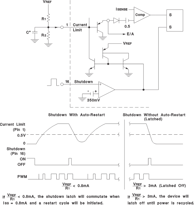 Figure 9. Soft-Start and Shutdown, Restart Functions
8.2.3 Application Curves
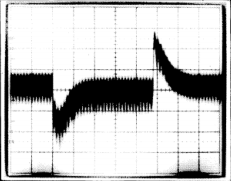
| t = 0.2 ms/div | output response = 20 mV/div | |
