SLUS352C January 1997 – December 2015 UC1846 , UC2846 , UC3846 , UC3847
PRODUCTION DATA.
- 1 Features
- 2 Applications
- 3 Description
- 4 Revision History
- 5 Pin Configuration and Functions
- 6 Specifications
- 7 Detailed Description
- 8 Application and Implementation
- 9 Power Supply Recommendations
- 10Layout
- 11Device and Documentation Support
- 12Mechanical, Packaging, and Orderable Information
パッケージ・オプション
デバイスごとのパッケージ図は、PDF版データシートをご参照ください。
メカニカル・データ(パッケージ|ピン)
- J|16
サーマルパッド・メカニカル・データ
発注情報
10 Layout
10.1 Layout Guidelines
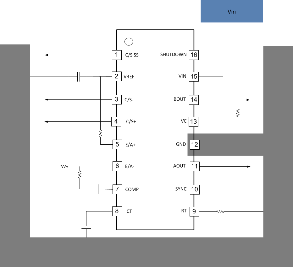
- Place a low ESR and ESL decoupling capacitor CREF in the 1-µF to 2.2-µF range, preferably ceramic, from VREF pin to GND.
- The EA+ is a non-inverting input, the EA– is an inverting input and the COMP is the output of the error amplifier. Place resistor and capacitor series network between EA+ pin and COMP pin, and reduce the trace of resistor and capacitor series network as much as possible.
- Place a low ESR and ESL capacitor CT, preferably ceramic, from CT pin to GND, and place CT close to UCx846/7 as much as possible.
- Place a resistor RT from RT pin to GND, and place RT close to UCx846/7 as much as possible.
10.2 Layout Example
 Figure 12. UCx84x Layout Example