SLUS191D February 1997 – July 2017 UC1525A , UC1527A , UC2525A , UC2527A , UC3525A , UC3527A
PRODUCTION DATA.
- 1 Features
- 2 Applications
- 3 Description
- 4 Revision History
- 5 Pin Configuration and Functions
- 6 Specifications
- 7 Detailed Description
- 8 Application and Implementation
- 9 Power Supply Recommendations
- 10Layout
- 11Device and Documentation Support
- 12Mechanical, Packaging, and Orderable Information
パッケージ・オプション
デバイスごとのパッケージ図は、PDF版データシートをご参照ください。
メカニカル・データ(パッケージ|ピン)
- N|16
サーマルパッド・メカニカル・データ
発注情報
1 Features
- 8-V to 35-V Operation
- 5.1-V Reference Trimmed to 1%
- 100-Hz to 500-kHz Oscillator Range
- Separate Oscillator Sync Terminal
- Adjustable Dead-Time Control
- Internal Soft Start
- Pulse-by-Pulse Shutdown
- Input Undervoltage Lockout With Hysteresis
- Latching PWM to Prevent Multiple Pulses
- Dual Source and Sink Output Drivers
2 Applications
- Off-Line and DC/DC Power Supplies
- Converters Using Voltage Mode
- Single-Ended or Two-Switch Topology Designs
- Solar Inverters
- Welding Inverters
- Motor Control
- Battery Chargers
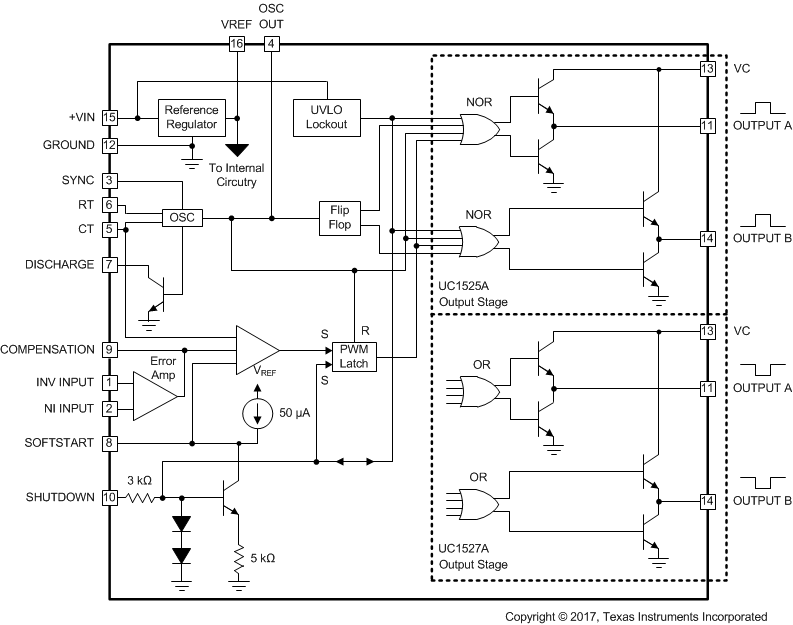
Block Diagram

3 Description
The UC1525A/1527A series of pulse width modulator integrated circuits are designed to offer improved performance and lowered external parts count when used in designing all types of switching power supplies. The on-chip 5.1-V reference is trimmed to 1% and the input common-mode range of the error amplifier includes the reference voltage, eliminating external resistors. A sync input to the oscillator allows multiple units to be slaved or a single unit to be synchronized to an external system clock. A single resistor between CT and the discharge terminals provides a wide range of dead-time adjustment. These devices also feature built-in soft-start circuitry with only an external timing capacitor required. A shutdown terminal controls both the soft-start circuitry and the output stages, providing instantaneous turn off through the PWM latch with pulsed shutdown, as well as soft-start recycle with longer shutdown commands.
Device Information(1)
| PART NUMBER | PACKAGE | BODY SIZE (NOM) |
|---|---|---|
| UCx52xA | LCCC (20) | 8.89 mm × 8.89 mm |
| CDIP (16) | 19.56 mm × 6.67 mm | |
| SOIC (16) | 10.30 mm × 7.50 mm | |
| PDIP (16) | 19.30 mm × 6.35 mm | |
| PLCC (20) | 8.96 mm × 8.96 mm |
- For all available packages, see the orderable addendum at the end of the data sheet.
4 Revision History
Changes from C Revision (January 2008) to D Revision
- Added ESD Ratings table, Feature Description section, Device Functional Modes, Application and Implementation section, Power Supply Recommendations section, Layout section, Device and Documentation Support section, and Mechanical, Packaging, and Orderable Information section Go
- Added Thermal Information tableGo
- Changed RθJA values in the Thermal Information table: from 80-120 to N/A for J; from 90 to 47.6 for N; from 45-90 to 72.6 for DW; from 43-75 to 55.8 for FN; and from 70-80 to N/A for FK Go
- Changed RθJC values in the Thermal Information table: from 28 to 37.4 (top) and 10.1 (bottom) for J; from 45 to 37.3 (top) for N; from 25 to 34 (top) for DW; from 34 to 33.7 (top) for FN; and from 20 to 32.9 (top) to 3.5 (bottom) for FK Go