JAJSQN3 june   2023  – june 2023 UCC14140-Q1

PRODUCTION DATA  

  1.   1
  2. 特長
  3. アプリケーション
  4. 概要
  5. Revision History
  6. Device Comparison
  7. Pin Configuration and Functions
  8. Specifications
    1. 7.1  Absolute Maximum Ratings
    2. 7.2  ESD Ratings
    3. 7.3  Recommended Operating Conditions
    4. 7.4  Thermal Information
    5. 7.5  Insulation Specifications
    6. 7.6  Safety-Related Certifications
    7. 7.7  Electrical Characteristics
    8. 7.8  Safety Limiting Values
    9. 7.9  Insulation Characteristics
    10. 7.10 Typical Characteristics
  9. Detailed Description
    1. 8.1 Overview
    2. 8.2 Functional Block Diagram
    3. 8.3 Feature Description
      1. 8.3.1 Power Stage Operation
        1. 8.3.1.1 VDD-VEE Voltage Regulation
        2. 8.3.1.2 COM-VEE Voltage Regulation
        3. 8.3.1.3 Power Handling Capability
      2. 8.3.2 Output Voltage Soft Start
      3. 8.3.3 ENA and PG
      4. 8.3.4 Protection Functions
        1. 8.3.4.1 Input Undervoltage Lockout
        2. 8.3.4.2 Input Overvoltage Lockout
        3. 8.3.4.3 Output Undervoltage Protection
        4. 8.3.4.4 Output Overvoltage Protection
        5. 8.3.4.5 Overpower Protection
        6. 8.3.4.6 Overtemperature Protection
    4. 8.4 Device Functional Modes
  10. Application and Implementation
    1. 9.1 Application Information
    2. 9.2 Typical Application
      1. 9.2.1 Design Requirements
      2. 9.2.2 Detailed Design Procedure
        1. 9.2.2.1 Capacitor Selection
        2. 9.2.2.2 Single RLIM Resistor Selection
        3. 9.2.2.3 RDR Circuit Component Selection
    3. 9.3 System Examples
    4. 9.4 Power Supply Recommendations
    5. 9.5 Layout
      1. 9.5.1 Layout Guidelines
      2. 9.5.2 Layout Example
  11. 10Device and Documentation Support
    1. 10.1 Documentation Support
      1. 10.1.1 Related Documentation
    2. 10.2 ドキュメントの更新通知を受け取る方法
    3. 10.3 サポート・リソース
    4. 10.4 Trademarks
    5. 10.5 静電気放電に関する注意事項
    6. 10.6 用語集
  12. 11Mechanical, Packaging, and Orderable Information

パッケージ・オプション

メカニカル・データ(パッケージ|ピン)
サーマルパッド・メカニカル・データ
発注情報

Insulation Characteristics

Insulation lifetime projection data is collected by using industry-standard Time Dependent Dielectric Breakdown (TDDB) test method. In this test, all pins on each side of the barrier are tied together creating a two-terminal device and high voltage applied between the two sides; The insulation breakdown data is collected at various high voltages switching at 60 Hz over temperature. For basic insulation, VDE standard requires the use of TDDB projection line with failure rate of less than 1000 part per million (ppm). Even though the expected minimum insulation lifetime is 20 years at the specified working isolation voltage, VDE basic certification requires additional safety margin of 20% for working voltage and 20% for lifetime which translates into minimum required insulation lifetime of 24 years at a working voltage that's 20% higher than the specified value. The TDDB projection line shows the intrinsic capability of the isolation barrier to withstand high voltage stress over its lifetime. Based on the TDDB data, the intrinsic capability of the insulation is 850 VRMS with a lifetime of >>100 years.
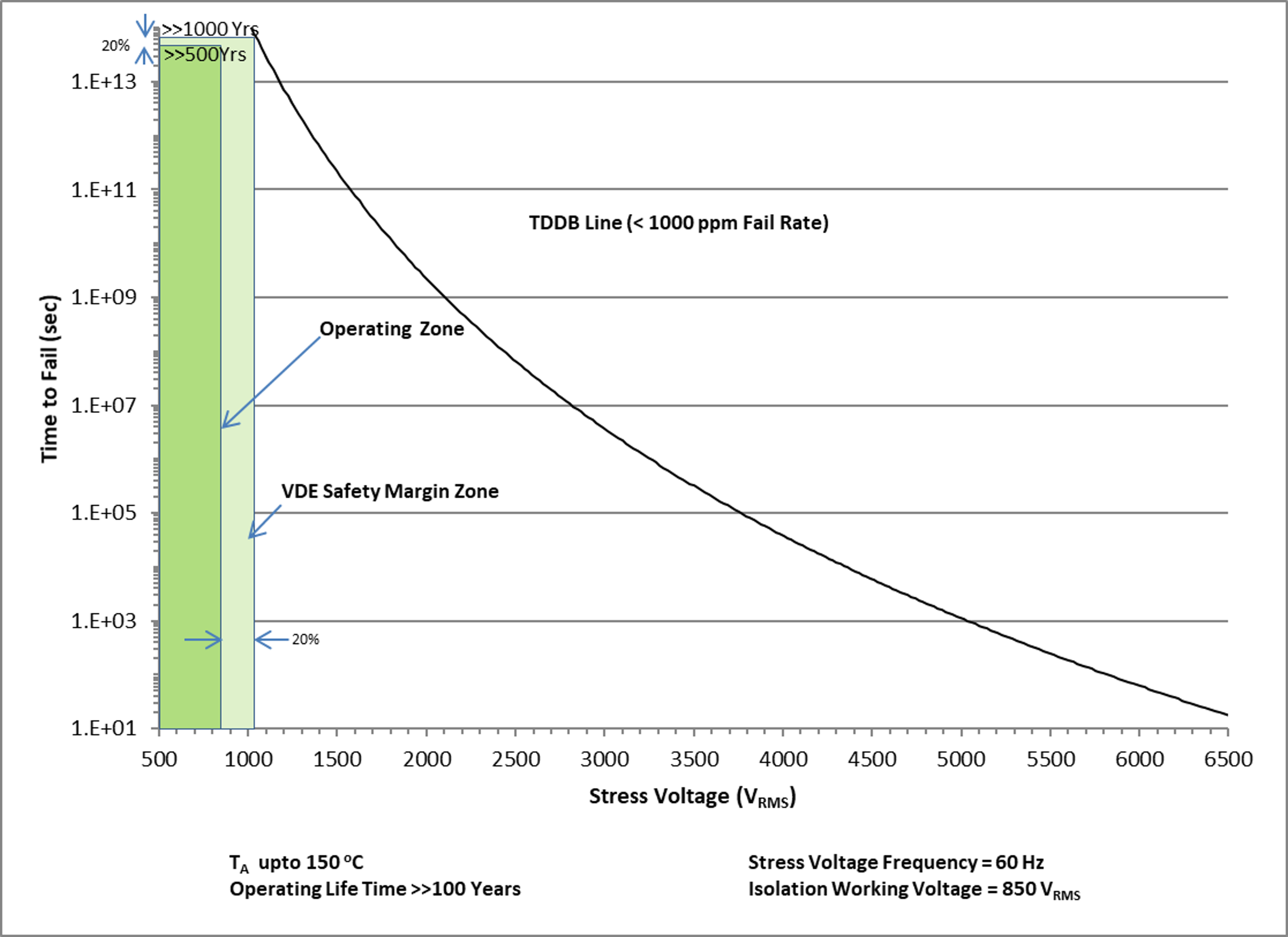
GUID-65829D2B-DDC3-4154-8367-B6D545409A93-low.png Figure 7-1 TDDB: Insulation Lifetime Projection for 850 Vrms Working Voltage.