JAJSQ36A april 2023 – august 2023 UCC14241-Q1
PRODUCTION DATA
- 1
- 1 特長
- 2 アプリケーション
- 3 概要
- 4 Revision History
- 5 Device Comparison
- 6 Pin Configuration and Functions
- 7 Specifications
- 8 Safety-Related Certifications
- 9 Insulation Characteristics
- 10Typical Characteristics
- 11Detailed Description
- 12Application and Implementation
- 13Device and Documentation Support
- 14Mechanical, Packaging, and Orderable Information
- 15Tape and Reel Information
9 Insulation Characteristics
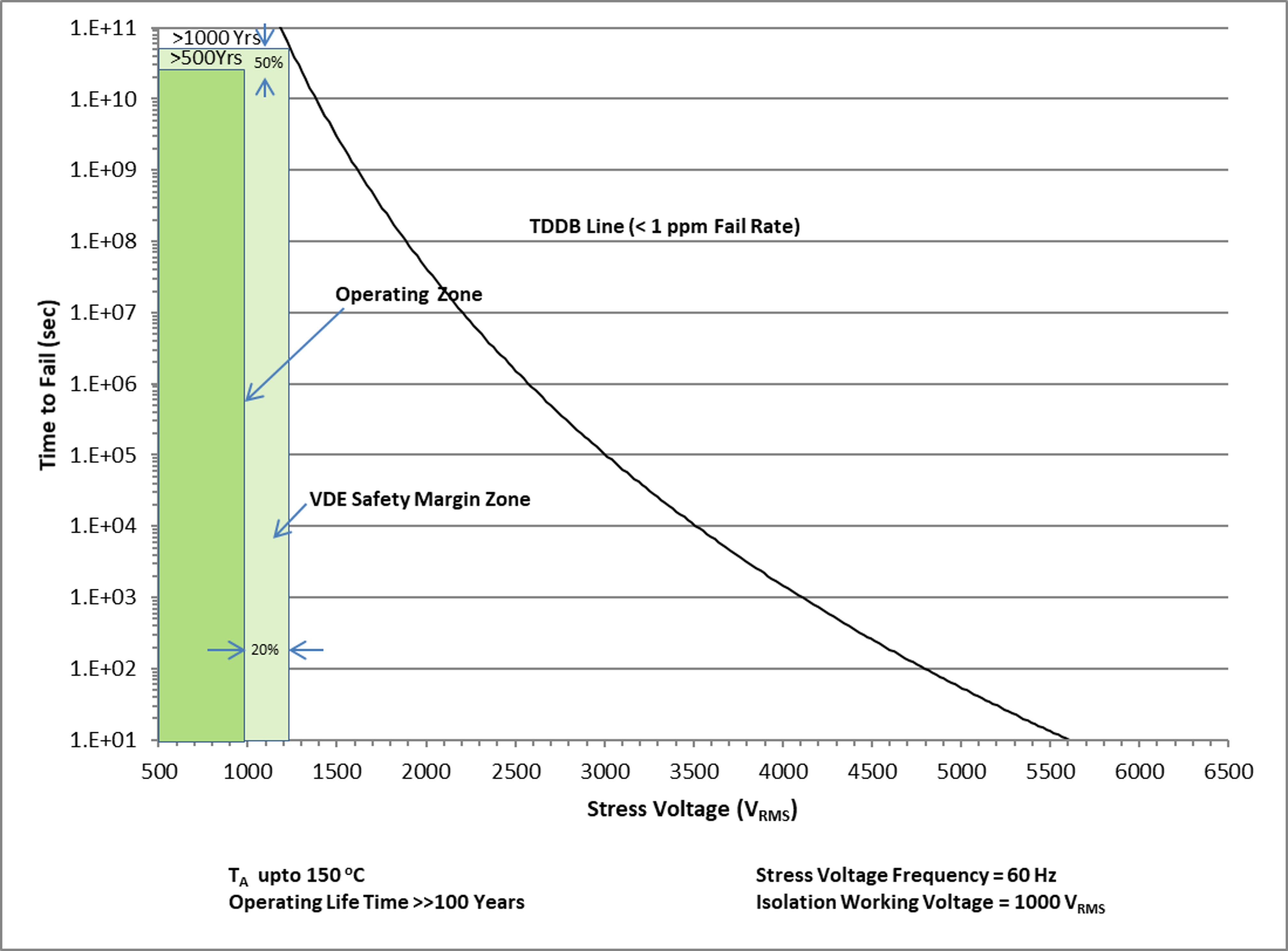
Insulation lifetime projection data is collected by using industry-standard Time Dependent Dielectric Breakdown (TDDB) test method. In this test, all pins on each side of the barrier are tied together creating a two-terminal device and high voltage applied between the two sides; The insulation breakdown data is collected at various high voltages switching at 60 Hz over temperature. For reinforced insulation, VDE standard requires the use of TDDB projection line with failure rate of less than 1 part per million (ppm). Even though the expected minimum insulation lifetime is 20 years at the specified working isolation voltage, VDE reinforce certification requires additional safety margin of 20% for working voltage and 50% for lifetime which translates into minimum required insulation lifetime of 30 years at a working voltage that's 20% higher than the specified value. The TDDB projection line shows the intrinsic capability of the isolation barrier to withstand high voltage stress over its lifetime. Based on the TDDB data, the intrinsic capability of the insulation is 1000 VRMS with a lifetime >>100 years.
 Figure 9-1 TDDB:
Insulation Lifetime Projection for 1000 Vrms Working Voltage.