JAJSR37A August 2023 – September 2023 UCC14340-Q1
PRODUCTION DATA
- 1
- 1 特長
- 2 アプリケーション
- 3 概要
- 4 Revision History
- 5 Device Comparison
- 6 Pin Configuration and Functions
- 7 Specifications
- 8 Detailed Description
- 9 Application and Implementation
- 10System Examples
- 11Power Supply Recommendations
- 12Layout
- 13デバイスおよびドキュメントのサポート
- 14Mechanical, Packaging, and Orderable Information
- 15Tape and Reel Information
12.1 Layout Guidelines
The UCC14340-Q1 integrated isolated power solution simplifies system design and reduces board area usage. Follow these guidelines for proper PCB layout to achieve optimum performance. A minimum of 4-layer PCB layer stack using 2-ounce copper on external layers is recommended to accomplish a good thermal PCB design.
- Input capacitors:
- Place the 0.1-µF high frequency bypass capacitor (C14) as close as possible to pins 6, 7 (VIN) and pins 8–18 (GNDP) and on the same side of the PCB as the IC. 0402 ceramic SMD or smaller is a desired size for optimal placement. Do not place any vias between the bypass capacitor and the IC pins so as to force the high frequency current through the capacitor.
- Place the bulk VIN capacitor(s) (C12, C13) as close as possible and parallel to the 0.1 µF high frequency bypass capacitor (C14) and on the same side of the PCB as the IC.
- Output capacitors:
- Place the 0.1-µF high frequency bypass capacitor (C7) as close as possible to pins 28, 29 (VDD) and pins 30, 31 (VEE) and on the same side of the PCB as the IC. 0402 ceramic SMD or smaller is a desired size for optimal placement. Do not place any vias between the bypass capacitor and the IC pins so as to force the high frequency current through the capacitor.
- Place the bulk VDD-VEE capacitor (C8) as close as possible and parallel to the
0.1-µF high frequency bypass capacitor (C7) and on the same side of the PCB as the
IC.
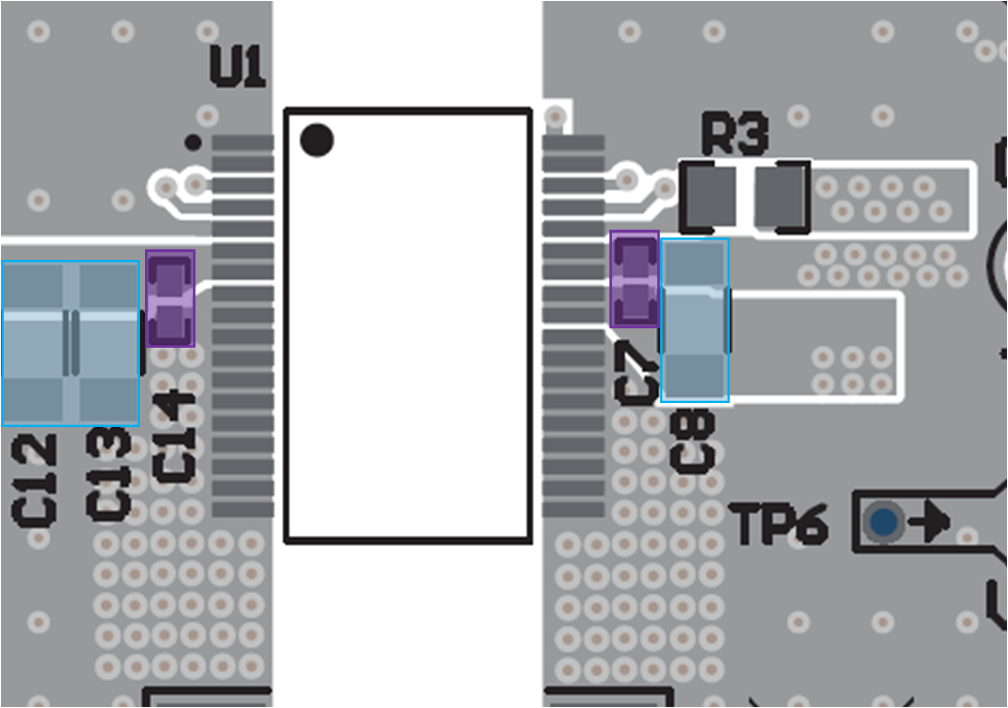 Figure 12-1
- Gate driver output capacitors: COUT2 and COUT3 are reference
designators referred to in the Excel calculator tool. COUT2 is the capacitor(s)
between VDD-COM and COUT3 is the capacitor(s) between COM-VEE. COUT2
and COUT3 are capacitors required by the gate driver IC. Proper selection and
component placement of COUT2 and COUT3 are critical for optimal
performance of the UCC14340-Q1 and the gate driver IC.
-
COUT2 and COUT3 should be placed next to the gate driver IC for best decoupling and gate driver switching performance
- Adding a COUT1B between VDD-VEE but placed at the gate driver in parallel with COUT2 and COUT3 will reduce the total capacitance needed and reduce the sensitivity to capacitor variation, and will allow to use a higher RLIM resistance value.
-
- RLIM: Place RLIM (R3) close to pin 32 and between the COM midpoint
of the output capacitive divider. The via pattern shown to the right of R3 connects to
COM.
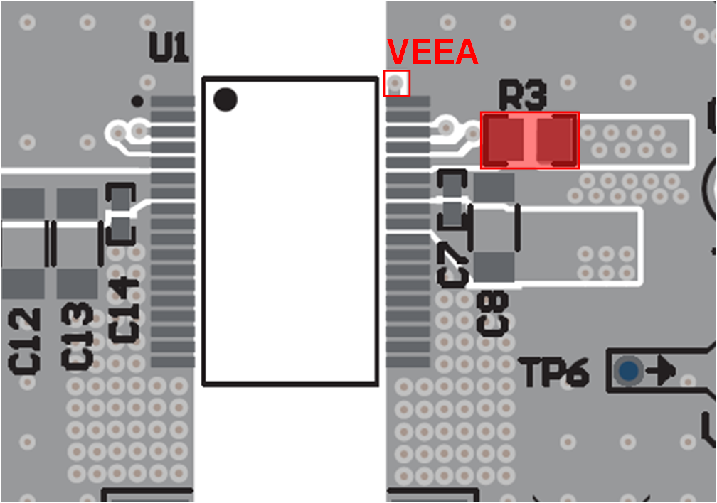 Figure 12-2
 -
Feedback:
-
VEEA (pin 35) should be isolated through all PCB layers, from the VEE plane as shown in the red box below. Use one via to make a direct connection to the FBVDD and FBVEE low-side resistors and capacitors (C15-16, R6-7), shown on the bottom side of the PCB.
-
Place feedback resistors (R4-7) and 330-pF ceramic capacitor in parallel with low-side resistors (R6-7) close to the IC preferably on the opposite side of IC (as shown in EVM), or on same layer as IC near pin 36.
-
The top-side feedback resistor should be placed next to the low-side resistor with a short, direct connection between both resistors and single connection to FBVDD. The top connection to sense the regulated rail (VDD-VEE) should be routed and connected at the VDD bias capacitor remote location near the gate driver pins for best accuracy and best transient response.
-
The top-side feedback resistor should be placed next to the low-side resistor with a short, direct connection between both resistors and single connection to FBVEE; while the top connection to sense the regulated rail (COM-VEE) should be routed and connected at the COM bias capacitor remote location near the gate driver pins for best accuracy and best transient response.
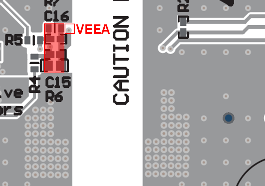 Figure 12-3
-
-
Thermal Vias: TheUCC14340-Q1 internal transformer makes a direct connection to the lead frame. It is therefore critical to provide adequate space and proper heatsinking designed into the PCB as outlined in the steps below.
-
TI recommends to connect the VIN, GNDP, VDD, and VEE pins to internal ground or power planes through multiple vias. Alternatively, make the polygons connected to these pins as wide as possible.
-
Use multiple thermal vias connecting PCB top side GNDP copper to bottom side GNDP copper. If possible, it is recommended to use 2-ounce copper on external top and bottom PCB layers.
-
Use multiple thermal vias connecting PCB top side VEE copper to bottom side VEE copper. If possible, it is recommended to use 2-ounce copper on external top and bottom PCB layers.
-
Thermal vias connecting top and bottom copper can also connect to internal copper layers for further improved heat extraction.
-
Thermal vias should be similar to pattern shown below but apply as many as the copper area will allow. The UCC14141EVM-068 uses thermal via arrays of approximately 220 mil x 350 mil (48 thermal vias on GNDP primary and 54 thermal vias on VEE secondary). Thermal via is 30 mil diameter, 12 mil hole size.
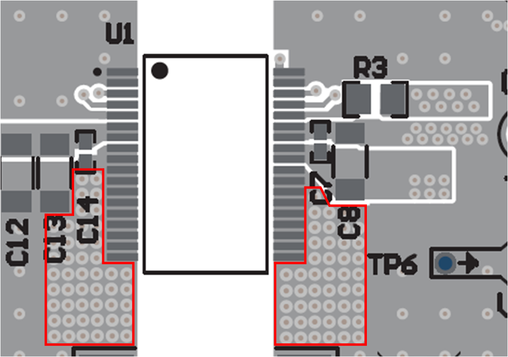 Figure 12-4
 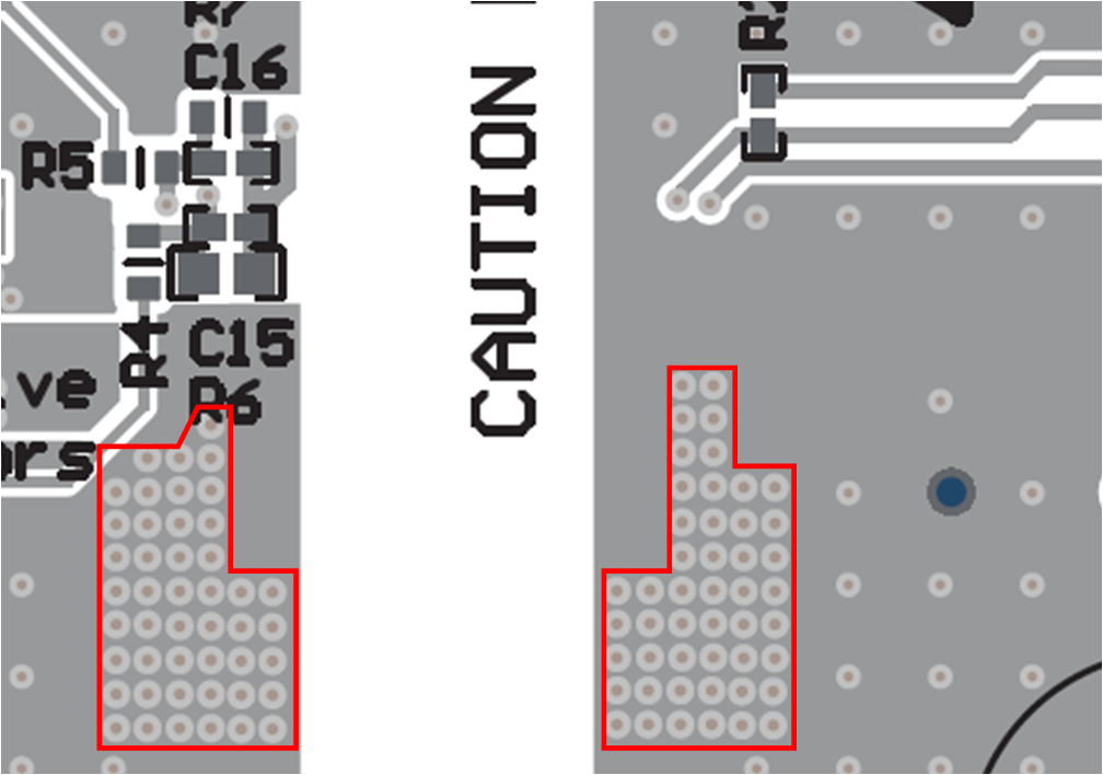 Figure 12-5
 -
As seen in the Thermal Image, there is a point of diminishing return, regarding the number of vias and size of the thermal via array. For 1.5-W of output power, heat transfer is shown to quickly diminish just beyond C12 and C8. The distance from the inner pad line of U1 to C12 is 320 mils.
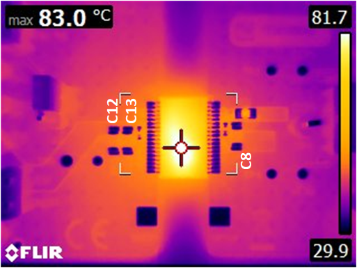 Figure 12-6 Thermal Image
 -
-
Creepage clearance: Avoid routing copper under the UCC14340-Q1 , to maintain the full creepage, clearance and basic voltage isolation ratings specified in the data sheet. Maintain the clearance width highlighted in red, throughout the entire defined isolation barrier. Keep-out clearance for basic isolation can be 50% less than the reinforced isolation requirement (8mm). Using 8mm provides additional margin.
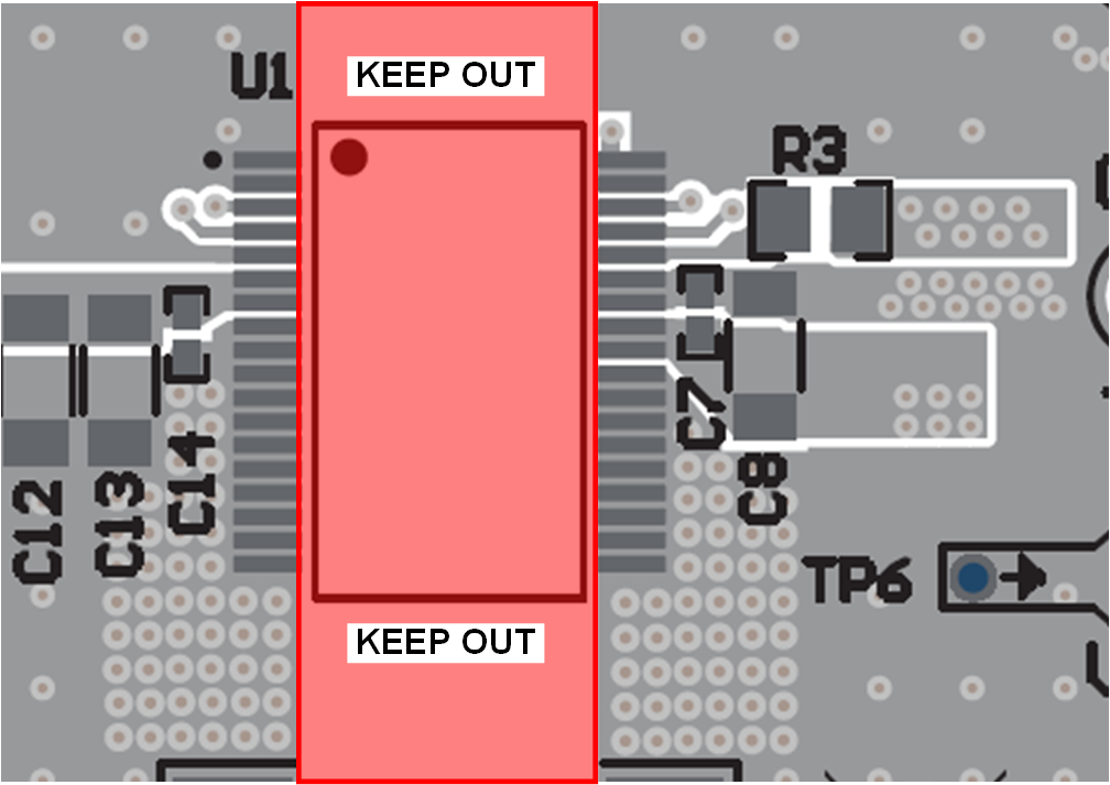 Figure 12-7
 -
Gate driver capacitors and feedback routing:
- VDD-COM and VEE-COM capacitors are populated on the UCC14141EVM-068 but these capacitors need to be placed as close to the associated gate driver pins as possible.
- For optimal voltage regulation, the feedback trace from COM (COM FB) and VDD (VDD
FB) should be as direct as possible so that the voltage feedback is being sensed
directly at the VDD and COM capacitors near the gate driver IC.
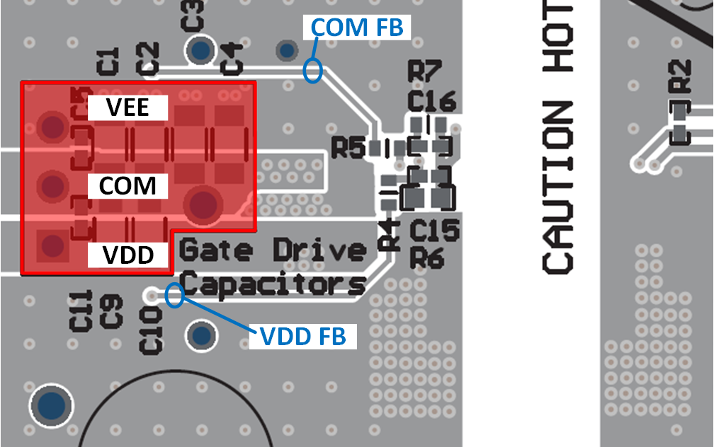 Figure 12-8