JAJSPV4C February   2023  – March 2024 UCC14341-Q1

PRODUCTION DATA  

  1.   1
  2. 特長
  3. アプリケーション
  4. 概要
  5. Device Comparison
  6. Pin Configuration and Functions
  7. Specifications
    1. 6.1  Absolute Maximum Ratings
    2. 6.2  ESD Ratings
    3. 6.3  Recommended Operating Conditions
    4. 6.4  Thermal Information
    5. 6.5  Insulation Specifications
    6. 6.6  Electrical Characteristics
    7. 6.7  Safety Limiting Values
    8. 6.8  Safety-Related Certifications
    9. 6.9  Insulation Characteristics
    10. 6.10 Typical Characteristics
  8. Detailed Description
    1. 7.1 Overview
    2. 7.2 機能ブロック図
    3. 7.3 Feature Description
      1. 7.3.1 Power Stage Operation
        1. 7.3.1.1 VDD-VEE Voltage Regulation
        2. 7.3.1.2 COM-VEE Voltage Regulation
        3. 7.3.1.3 Power Handling Capability
      2. 7.3.2 Output Voltage Soft Start
      3. 7.3.3 ENA and PG
      4. 7.3.4 Protection Functions
        1. 7.3.4.1 Input Undervoltage Lockout
        2. 7.3.4.2 Input Overvoltage Lockout
        3. 7.3.4.3 Output Undervoltage Protection
        4. 7.3.4.4 Output Overvoltage Protection
        5. 7.3.4.5 Overpower Protection
        6. 7.3.4.6 Over-Temperature Protection
    4. 7.4 Device Functional Modes
  9. Application and Implementation
    1. 8.1 Application Information
    2. 8.2 Typical Application
      1. 8.2.1 Design Requirements
      2. 8.2.2 Detailed Design Procedure
        1. 8.2.2.1 Capacitor Selection
        2. 8.2.2.2 Single RLIM Resistor Selection
        3. 8.2.2.3 RDR Circuit Component Selection
        4. 8.2.2.4 Feedback Resistors Selection
    3. 8.3 System Examples
    4. 8.4 Power Supply Recommendations
    5. 8.5 Layout
      1. 8.5.1 Layout Guidelines
      2. 8.5.2 Layout Example
  10. デバイスおよびドキュメントのサポート
    1. 9.1 ドキュメントのサポート
      1. 9.1.1 関連資料
    2. 9.2 ドキュメントの更新通知を受け取る方法
    3. 9.3 サポート・リソース
    4. 9.4 商標
    5. 9.5 静電気放電に関する注意事項
    6. 9.6 用語集
  11. 10Revision History
  12. 11Mechanical, Packaging, and Orderable Information
  13. 12Tape and Reel Information

パッケージ・オプション

メカニカル・データ(パッケージ|ピン)
サーマルパッド・メカニカル・データ
発注情報

Layout Example

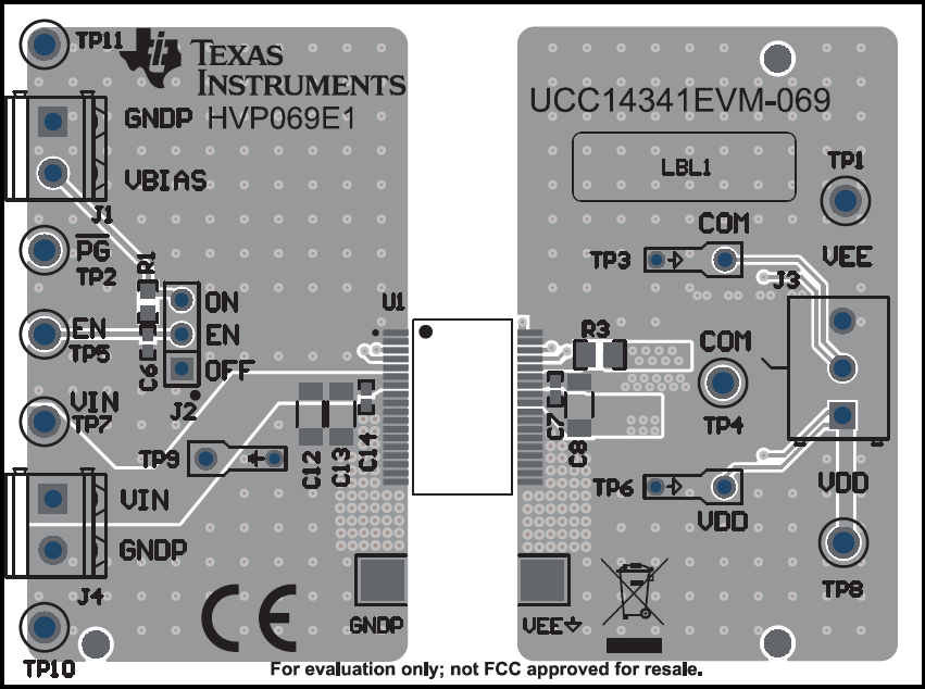
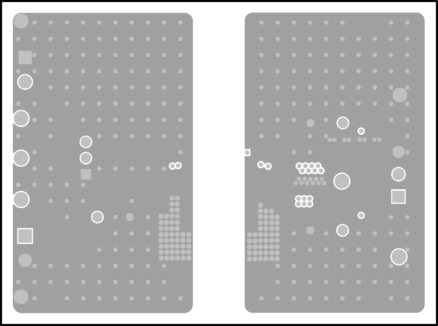
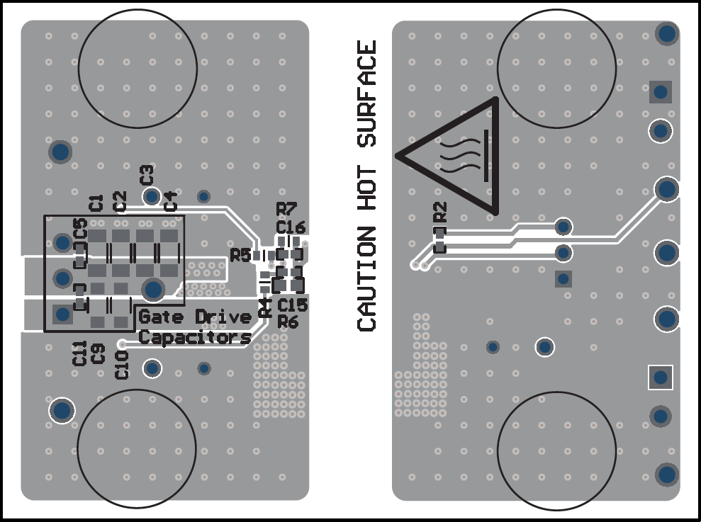
The layout example shown in the following figures is from the evaluation board UCC14341-Q1EVM, UCC14341EVM-069, and based on the Figure 8-8 design.

GUID-559E9A4F-0239-4349-9189-2600FE997BEA-low.png

Figure 8-21 UCC14341-Q1EVM, PCB Top Layer, Assembly

GUID-456F44CE-B8BA-4074-92A1-D3FD8E760A7A-low.png

Figure 8-22 UCC14341-Q1EVM, Signal Layer 2 (Same as Layer 3)
GUID-26B568FC-733C-41F5-9FA2-7DF996646B9C-low.png

Figure 8-23 UCC14341-Q1EVM, Signal Layer 3 (Same as Layer 2)
GUID-5D1161F8-5B23-4C78-8BE4-AEC87EE3E561-low.png

Figure 8-24 UCC14341-Q1EVM, PCB Bottom Layer, Assembly (Mirrored View)