JAJSEW6B February   2018  – February 2024 UCC21222

PRODUCTION DATA  

  1.   1
  2. 特長
  3. アプリケーション
  4. 概要
  5. Pin Configuration and Functions
  6. Specifications
    1. 5.1  Absolute Maximum Ratings
    2. 5.2  ESD Ratings
    3. 5.3  Recommended Operating Conditions
    4. 5.4  Thermal Information
    5. 5.5  Power Ratings
    6. 5.6  Insulation Specifications
    7. 5.7  Safety-Related Certifications
    8. 5.8  Safety-Limiting Values
    9. 5.9  Electrical Characteristics
    10. 5.10 Switching Characteristics
    11. 5.11 Thermal Derating Curves
    12. 5.12 Typical Characteristics
  7. Parameter Measurement Information
    1. 6.1 Minimum Pulses
    2. 6.2 Propagation Delay and Pulse Width Distortion
    3. 6.3 Rising and Falling Time
    4. 6.4 Input and Disable Response Time
    5. 6.5 Programmable Dead Time
    6. 6.6 Power-Up UVLO Delay to OUTPUT
    7. 6.7 CMTI Testing
  8. Detailed Description
    1. 7.1 Overview
    2. 7.2 Functional Block Diagram
    3. 7.3 Feature Description
      1. 7.3.1 VDD, VCCI, and Undervoltage Lock Out (UVLO)
      2. 7.3.2 Input and Output Logic Table
      3. 7.3.3 Input Stage
      4. 7.3.4 Output Stage
      5. 7.3.5 Diode Structure in the UCC21222
    4. 7.4 Device Functional Modes
      1. 7.4.1 Disable Pin
      2. 7.4.2 Programmable Dead Time (DT) Pin
        1. 7.4.2.1 DT Pin Tied to VCCI or DT Pin Left Open
        2. 7.4.2.2 Connecting a Programming Resistor between DT and GND Pins
  9. Application and Implementation
    1. 8.1 Application Information
    2. 8.2 Typical Application
      1. 8.2.1 Design Requirements
      2. 8.2.2 Detailed Design Procedure
        1. 8.2.2.1 Custom Design With WEBENCH® Tools
        2. 8.2.2.2 Designing INA/INB Input Filter
        3. 8.2.2.3 Select Dead Time Resistor and Capacitor
        4. 8.2.2.4 Select External Bootstrap Diode and its Series Resistor
        5. 8.2.2.5 Gate Driver Output Resistor
        6. 8.2.2.6 Estimating Gate Driver Power Loss
        7. 8.2.2.7 Estimating Junction Temperature
        8. 8.2.2.8 Selecting VCCI, VDDA/B Capacitor
          1. 8.2.2.8.1 Selecting a VCCI Capacitor
          2. 8.2.2.8.2 Selecting a VDDA (Bootstrap) Capacitor
          3. 8.2.2.8.3 Select a VDDB Capacitor
        9. 8.2.2.9 Application Circuits with Output Stage Negative Bias
      3. 8.2.3 Application Curves
  10. Power Supply Recommendations
  11. 10Layout
    1. 10.1 Layout Guidelines
      1. 10.1.1 Component Placement Considerations
      2. 10.1.2 Grounding Considerations
      3. 10.1.3 High-Voltage Considerations
      4. 10.1.4 Thermal Considerations
    2. 10.2 Layout Example
  12. 11Device and Documentation Support
    1. 11.1 Device Support
      1. 11.1.1 サード・パーティ製品に関する免責事項
      2. 11.1.2 Development Support
        1. 11.1.2.1 Custom Design With WEBENCH® Tools
    2. 11.2 Documentation Support
      1. 11.2.1 Related Documentation
    3. 11.3 ドキュメントの更新通知を受け取る方法
    4. 11.4 サポート・リソース
    5. 11.5 Trademarks
    6. 11.6 静電気放電に関する注意事項
    7. 11.7 用語集
  13. 12Revision History
  14. 13Mechanical, Packaging, and Orderable Information

パッケージ・オプション

メカニカル・データ(パッケージ|ピン)
サーマルパッド・メカニカル・データ
発注情報

Typical Characteristics

VDDA = VDDB = 12 V, VCCI = 3.3 V or 5.0 V, DT pin tied to VCCI, TA = 25°C, CL = 0 pF unless otherwise noted.
GUID-58AF1981-F509-4A8C-81A3-4686986E8E90-low.gif
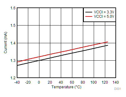
No Load INA = INB = GND
Figure 5-3 VCCI Quiescent Current
GUID-62D6249E-176B-49E9-8C15-F6784BAF9DED-low.gif
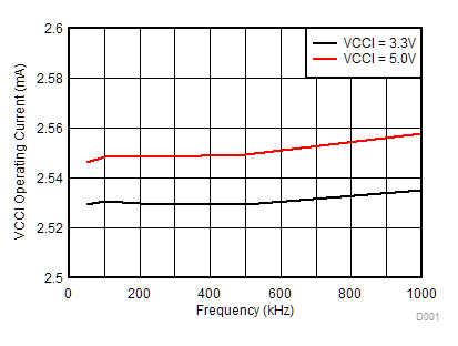
Figure 5-5 VCCI Operating Current vs. Frequency
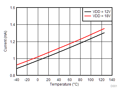
GUID-F1E11653-DD78-4294-B9B3-FCA86E83B9BC-low.gif
No Load
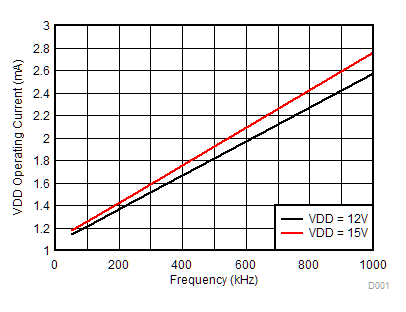
Figure 5-7 VDD Per Channel Operating Current - IVDDA/B
GUID-43721FA3-C5CF-4C9E-91F4-346E45CF39DB-low.gif
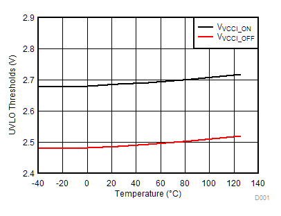
Figure 5-9 VCCI UVLO Threshold Voltage
GUID-814331E9-2990-4BA9-BBDA-CAF7913BD3AE-low.gif
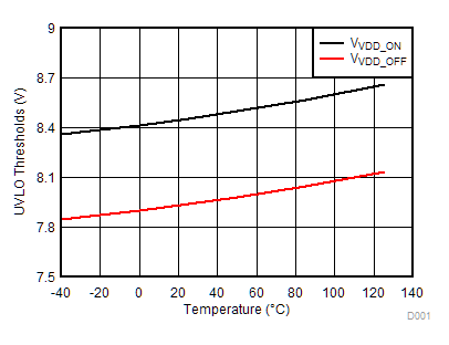
Figure 5-11 VDD UVLO Threshold Voltage
GUID-D4DBD2A1-4DD2-46F6-9360-4C48A2149C37-low.gif
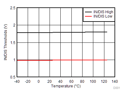
Figure 5-13 INA/INB/DIS High and Low Threshold Voltage
GUID-C064E26C-0D18-45B4-8B09-0CF4F6C752B4-low.gif
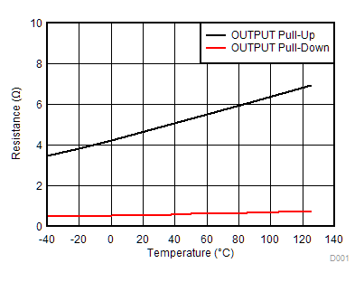
Figure 5-15 OUT Pullup and Pulldown Resistance
GUID-73FBA543-ADFC-4B84-B689-6FBE65ED1379-low.gif
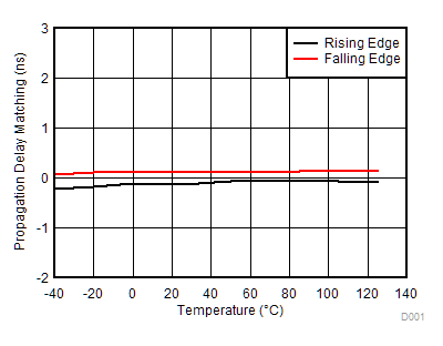
Figure 5-17 Propagation Delay Matching, Rising and Falling Edge
GUID-464FFECC-59B1-4BB0-9943-3B5828699592-low.gif
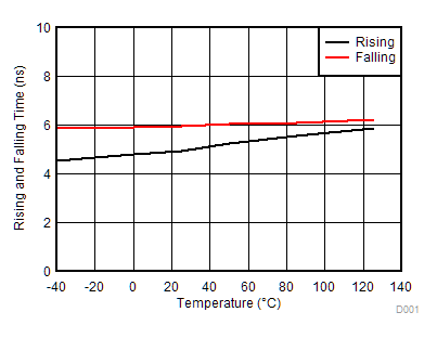
CL = 1.8 nF
Figure 5-19 Rise Time and Fall Time
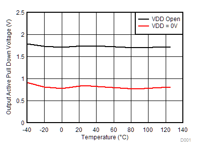
GUID-BCD3BF94-64E2-4D89-8B41-4354724D7808-low.gif
Figure 5-21 OUTPUT Active Pulldown Voltage
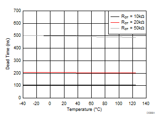
GUID-FBC6EC52-6ED1-4834-80D4-6BF35426E73B-low.gif
Figure 5-23 Dead Time Temperature Drift
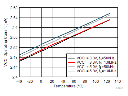
GUID-6FBDC40D-AE8A-444D-AD70-86E2988C7D0B-low.gif
Figure 5-4 VCCI Operating Current - IVCCI
GUID-674848C6-F153-4914-BE08-F003378ED5B8-low.gif
No Load INA = INB = GND
Figure 5-6 VDD Per Channel Quiescent Current (IVDDA, IVDDB)
GUID-2AAA89C5-719C-4053-8B63-80BDE75C68EA-low.gif
No Load INA and INB both switching
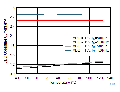
Figure 5-8 Per Channel Operating Current (IVDDA/B) vs. Frequency
GUID-B52ABF48-65AE-4707-82F2-F5C4E919212D-low.gif
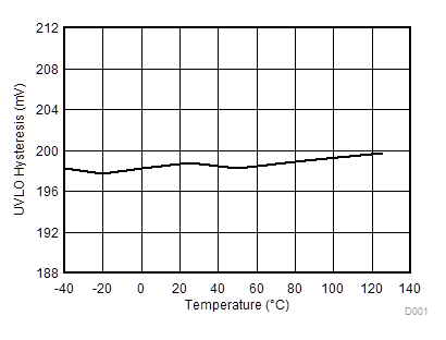
Figure 5-10 VCCI UVLO Threshold Hysteresis Voltage
GUID-61C38D46-F166-45E8-9AE3-B127B14FD994-low.gif
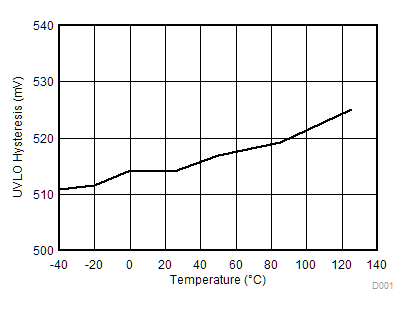
Figure 5-12 VDD UVLO Threshold Hysteresis Voltage
GUID-DCEAAB12-9D0F-4485-814D-516477BCB11C-low.gif
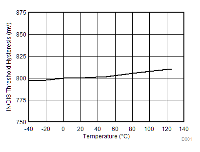
Figure 5-14 INA/INB/DIS High and Low Threshold Hysteresis
GUID-B1E8569A-7095-4CA3-98A8-F180265B7B4D-low.gif
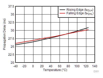
Figure 5-16 Propagation Delay, Rising and Falling Edge
GUID-44EB1797-82CA-4B8E-A97C-DD7238A0C9AD-low.gif
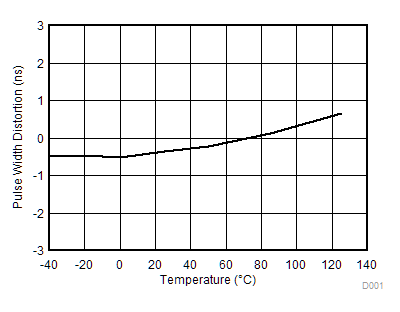
tPDLH – tPDHL
Figure 5-18 Pulse Width Distortion
GUID-335CA38D-45D6-4B2C-B9BC-F84A0101E936-low.gif
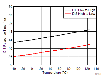
Figure 5-20 DISABLE Response Time
GUID-6C106D8F-4DE2-47B2-9530-F59A57982564-low.gif
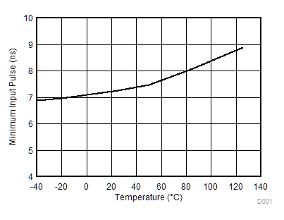
Figure 5-22 Minimum Pulse that Changes Output
GUID-5A74C919-9D6D-4B1F-9653-FF929EE50704-low.gif
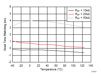
Figure 5-24 Dead Time Matching