JAJSE13E October 2017 – June 2024 UCC21520-Q1
PRODUCTION DATA
- 1
- 1 特長
- 2 アプリケーション
- 3 概要
- 4 Pin Configuration and Functions
-
5 Specifications
- 5.1 Absolute Maximum Ratings
- 5.2 ESD Ratings (Automotive)
- 5.3 Recommended Operating Conditions
- 5.4 Thermal Information
- 5.5 Power Ratings
- 5.6 Insulation Specifications
- 5.7 Safety Limiting Values
- 5.8 Electrical Characteristics
- 5.9 Timing Requirements
- 5.10 Switching Characteristics
- 5.11 Insulation Characteristics Curves
- 5.12 Typical Characteristics
- 6 Parameter Measurement Information
- 7 Detailed Description
-
8 Application and Implementation
- 8.1 Application Information
- 8.2
Typical Application
- 8.2.1 Design Requirements
- 8.2.2
Detailed Design Procedure
- 8.2.2.1 Designing INA/INB Input Filter
- 8.2.2.2 Select External Bootstrap Diode and its Series Resistor
- 8.2.2.3 Gate Driver Output Resistor
- 8.2.2.4 Gate to Source Resistor Selection
- 8.2.2.5 Estimate Gate Driver Power Loss
- 8.2.2.6 Estimating Junction Temperature
- 8.2.2.7 Selecting VCCI, VDDA/B Capacitor
- 8.2.2.8 Dead Time Setting Guidelines
- 8.2.2.9 Application Circuits with Output Stage Negative Bias
- 8.2.3 Application Curves
- 9 Power Supply Recommendations
- 10Layout
- 11Device and Documentation Support
- 12Revision History
- 13Mechanical, Packaging, and Orderable Information
パッケージ・オプション
メカニカル・データ(パッケージ|ピン)
- DW|16
サーマルパッド・メカニカル・データ
- DW|16
発注情報
8.2.2.9 Application Circuits with Output Stage Negative Bias
When parasitic inductances are introduced by non-ideal PCB layout and long package leads (for example, TO-220 and TO-247 type packages), there could be ringing in the gate-source drive voltage of the power transistor during high di/dt and dv/dt switching. If the ringing is over the threshold voltage, there is the risk of unintended turn-on and even shoot-through. Applying a negative bias on the gate drive is a popular way to keep such ringing below the threshold. Below are a few examples of implementing negative gate drive bias.
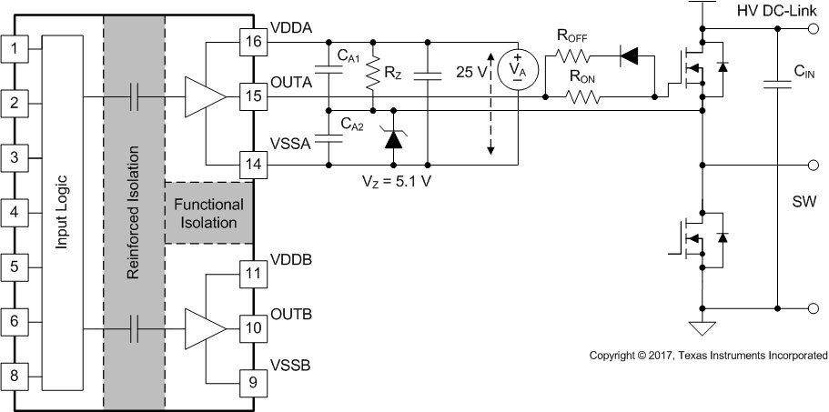
Figure 8-2 shows the first example with negative bias turn-off on the channel-A driver using a Zener diode on the isolated power supply output stage. The negative bias is set by the Zener diode voltage. If the isolated power supply, VA, is equal to 25 V, the turn-off voltage will be –5.1 V and turn-on voltage will be 25 V – 5.1 V ≈ 20 V. The channel-B driver circuit is the same as channel-A, therefore, this configuration needs two power supplies for a half-bridge configuration, and there will be steady state power consumption from RZ.
 Figure 8-2 Negative Bias with Zener Diode on Iso-Bias Power Supply
Output
Figure 8-2 Negative Bias with Zener Diode on Iso-Bias Power Supply
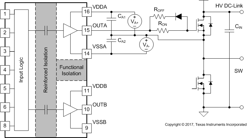
OutputFigure 8-3 shows another example which uses two supplies (or single-input-double-output power supply). Power supply VA+ determines the positive drive output voltage and VA– determines the negative turn-off voltage. The configuration for channel B is the same as channel A. This solution requires more power supplies than the first example, however, it provides more flexibility when setting the positive and negative rail voltages.
 Figure 8-3 Negative
Bias with Two Iso-Bias Power Supplies
Figure 8-3 Negative
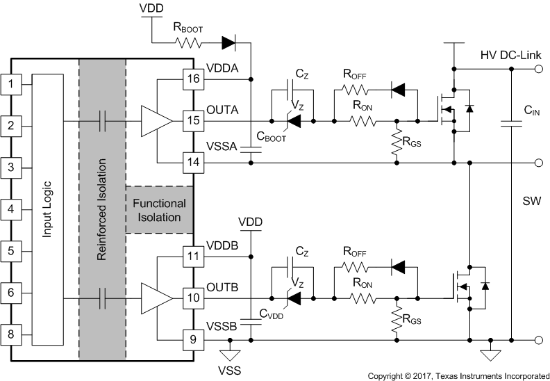
Bias with Two Iso-Bias Power SuppliesThe last example, shown in Figure 8-4, is a single power supply configuration and generates negative bias through a Zener diode in the gate drive loop. The benefit of this solution is that it only uses one power supply and the bootstrap power supply can be used for the high side drive. This design requires the least cost and design effort among the three solutions. However, this solution has limitations:
- The negative gate drive bias is not only determined by the Zener diode, but also by the duty cycle, which means the negative bias voltage will change when the duty cycle changes. Therefore, converters with a fixed duty cycle (~50%) such as variable frequency resonant convertors or phase shift convertors favor this solution.
- The high side VDDA-VSSA must maintain enough voltage to stay in the recommended power supply range, which means the low side switch must turn-on or have free-wheeling current on the body (or anti-parallel) diode for a certain period during each switching cycle to refresh the bootstrap capacitor. Therefore, a 100% duty cycle for the high side is not possible unless there is a dedicated power supply for the high side, like in the other two example circuits.
 Figure 8-4 Negative Bias with Single Power Supply and Zener Diode in Gate Drive
Path