JAJSQ94D January 2019 – June 2024 UCC21710-Q1
PRODUCTION DATA
- 1
- 1 特長
- 2 アプリケーション
- 3 概要
- 4 Pin Configuration and Functions
-
5 Specifications
- 5.1 Absolute Maximum Ratings
- 5.2 ESD Ratings
- 5.3 Recommended Operating Conditions
- 5.4 Thermal Information
- 5.5 Power Ratings
- 5.6 Insulation Specifications
- 5.7 Safety-Related Certifications
- 5.8 Safety Limiting Values
- 5.9 Electrical Characteristics
- 5.10 Switching Characteristics
- 5.11 Insulation Characteristics Curves
- 5.12 Typical Characteristics
- 6 Parameter Measurement Information
-
7 Detailed Description
- 7.1 Overview
- 7.2 Functional Block Diagram
- 7.3
Feature Description
- 7.3.1 Power Supply
- 7.3.2 Driver Stage
- 7.3.3 VCC and VDD Undervoltage Lockout (UVLO)
- 7.3.4 Active Pulldown
- 7.3.5 Short Circuit Clamping
- 7.3.6 Internal Active Miller Clamp
- 7.3.7 Overcurrent and Short Circuit Protection
- 7.3.8 Soft Turn-off
- 7.3.9 Fault ( FLT, Reset and Enable ( RST/EN)
- 7.3.10 Isolated Analog to PWM Signal Function
- 7.4 Device Functional Modes
-
8 Applications and Implementation
- 8.1 Application Information
- 8.2
Typical Application
- 8.2.1 Design Requirements
- 8.2.2
Detailed Design Procedure
- 8.2.2.1 Input filters for IN+, IN- and RST/EN
- 8.2.2.2 PWM Interlock of IN+ and IN-
- 8.2.2.3 FLT, RDY and RST/EN Pin Circuitry
- 8.2.2.4 RST/EN Pin Control
- 8.2.2.5 Turn on and turn off gate resistors
- 8.2.2.6 Overcurrent and Short Circuit Protection
- 8.2.2.7 Isolated Analog Signal Sensing
- 8.2.2.8 Higher Output Current Using an External Current Buffer
- 9 Power Supply Recommendations
- 10Layout
- 11Device and Documentation Support
- 12Revision History
- 13Mechanical, Packaging, and Orderable Information
パッケージ・オプション
メカニカル・データ(パッケージ|ピン)
- DW|16
サーマルパッド・メカニカル・データ
- DW|16
発注情報
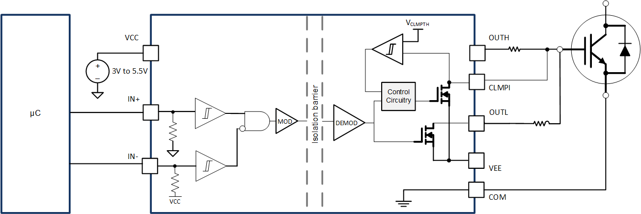
7.3.6 Internal Active Miller Clamp
Active miller clamp feature is important to prevent the false turn-on while the driver is in OFF state. In applications which the device can be in synchronous rectifier mode, the body diode conducts the current during the deadtime while the device is in OFF state, the drain-source or collector-emitter voltage remains the same and the dV/dt happens when the other power semiconductor of the phase leg turns on. The low internal pull-down impedance of UCC21710-Q1 can provide a strong pulldown to hold the OUTL to VEE. However, external gate resistance is usually adopted to limit the dV/dt. The miller effect during the turn on transient of the other power semiconductor can cause a voltage drop on the external gate resistor, which boost the gate-source or gate-emitter voltage. If the voltage on VGS or VGE is higher than the threshold voltage of the power semiconductor, a shoot through can happen and cause catastrophic damage. The active miller clamp feature of UCC21710-Q1 drives an internal MOSFET, which connects to the device gate. The internal MOSFET is triggered when the gate voltage is lower than VCLMPTH, which is 2V above VEE, and creates a low impedance path to avoid the false turn on issue.
 Figure 7-4 Active Miller Clamp