JAJSQ94C january 2019 – may 2023 UCC21710-Q1
PRODUCTION DATA
- 1
- 1 特長
- 2 アプリケーション
- 3 概要
- 4 Revision History
- 5 Pin Configuration and Functions
-
6 Specifications
- 6.1 Absolute Maximum Ratings
- 6.2 ESD Ratings
- 6.3 Recommended Operating Conditions
- 6.4 Thermal Information
- 6.5 Power Ratings
- 6.6 Insulation Specifications
- 6.7 Safety-Related Certifications
- 6.8 Safety Limiting Values
- 6.9 Electrical Characteristics
- 6.10 Switching Characteristics
- 6.11 Insulation Characteristics Curves
- 6.12 Typical Characteristics
- 7 Parameter Measurement Information
-
8 Detailed Description
- 8.1 Overview
- 8.2 Functional Block Diagram
- 8.3
Feature Description
- 8.3.1 Power Supply
- 8.3.2 Driver Stage
- 8.3.3 VCC and VDD Undervoltage Lockout (UVLO)
- 8.3.4 Active Pulldown
- 8.3.5 Short Circuit Clamping
- 8.3.6 Internal Active Miller Clamp
- 8.3.7 Overcurrent and Short Circuit Protection
- 8.3.8 Soft Turn-off
- 8.3.9 Fault ( FLT, Reset and Enable ( RST/EN)
- 8.3.10 Isolated Analog to PWM Signal Function
- 8.4 Device Functional Modes
-
9 Applications and Implementation
- 9.1 Application Information
- 9.2
Typical Application
- 9.2.1 Design Requirements
- 9.2.2
Detailed Design Procedure
- 9.2.2.1 Input filters for IN+, IN- and RST/EN
- 9.2.2.2 PWM Interlock of IN+ and IN-
- 9.2.2.3 FLT, RDY and RST/EN Pin Circuitry
- 9.2.2.4 RST/EN Pin Control
- 9.2.2.5 Turn on and turn off gate resistors
- 9.2.2.6 Overcurrent and Short Circuit Protection
- 9.2.2.7 Isolated Analog Signal Sensing
- 9.2.2.8 Higher Output Current Using an External Current Buffer
- 10Power Supply Recommendations
- 11Layout
- 12Device and Documentation Support
- 13Mechanical, Packaging, and Orderable Information
パッケージ・オプション
メカニカル・データ(パッケージ|ピン)
- DW|16
サーマルパッド・メカニカル・データ
- DW|16
発注情報
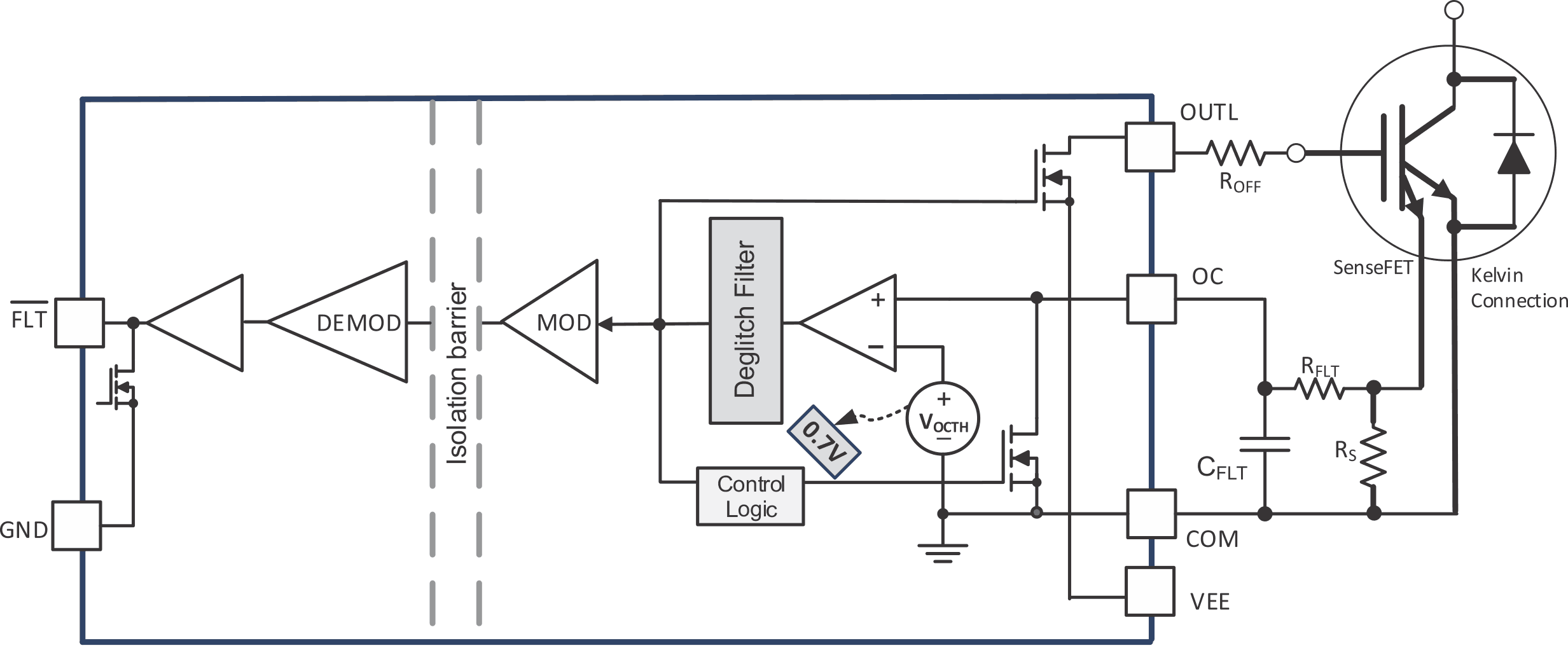
9.2.2.6.1 Protection Based on Power Modules with Integrated SenseFET
The overcurrent and short circuit protection function is suitable for the SiC MOSFET and IGBT modules with integrated SenseFET. The SenseFET scales down the main power loop current and outputs the current with a dedicated pin of the power module. With external high precision sensing resistor, the scaled down current can be measured and the main power loop current can be calculated. The value of the sensing resistor RS sets the protection threshold of the main current. For example, with a ratio of 1:N = 1:50000 of the integrated current mirror, by using the RS as 20Ω, the threshold protection current is:

The overcurrent and short circuit protection based on integrated SenseFET has high precision, as it is sensing the current directly. The accuracy of the method is related to two factors: the scaling down ratio of the main power loop current and the SenseFET, and the precision of the sensing resistor. Since the current is sensed from the SenseFET, which is isolated from the main power loop, and the current is scaled down significantly with much less dI/dt, the sensing loop has good noise immunity. To further improve the noise immunity, a low pass filter can be added. A 100pF to 10nF filter capacitor can be added. The delay time caused by the low pass filter should also be considered for the protection circuitry design.
 Figure 9-7 Overcurrent and Short Circuit
Protection Based on IGBT Module with SenseFET