JAJSJG8B August 2020 – February 2024 UCC21759-Q1
PRODUCTION DATA
- 1
- 1 特長
- 2 アプリケーション
- 3 概要
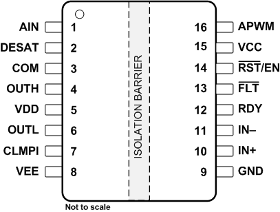
- 4 Pin Configuration and Functions
-
5 Specifications
- 5.1 Absolute Maximum Ratings
- 5.2 ESD Ratings
- 5.3 Recommended Operating Conditions
- 5.4 Thermal Information
- 5.5 Power Ratings
- 5.6 Insulation Specifications
- 5.7 Safety-Related Certifications
- 5.8 Safety Limiting Values
- 5.9 Electrical Characteristics
- 5.10 Switching Characteristics
- 5.11 Insulation Characteristics Curves
- 5.12 Typical Characteristics
- 6 Parameter Measurement Information
-
7 Detailed Description
- 7.1 Overview
- 7.2 Functional Block Diagram
- 7.3
Feature Description
- 7.3.1 Power Supply
- 7.3.2 Driver Stage
- 7.3.3 VCC and VDD Undervoltage Lockout (UVLO)
- 7.3.4 Active Pulldown
- 7.3.5 Short Circuit Clamping
- 7.3.6 Internal Active Miller Clamp
- 7.3.7 Desaturation (DESAT) Protection
- 7.3.8 Soft Turn-off
- 7.3.9 Fault ( FLT, Reset and Enable ( RST/EN)
- 7.3.10 Isolated Analog to PWM Signal Function
- 7.4 Device Functional Modes
-
8 Applications and Implementation
- 8.1 Application Information
- 8.2
Typical Application
- 8.2.1 Design Requirements
- 8.2.2
Detailed Design Procedure
- 8.2.2.1 Input filters for IN+, IN- and RST/EN
- 8.2.2.2 PWM Interlock of IN+ and IN-
- 8.2.2.3 FLT, RDY and RST/EN Pin Circuitry
- 8.2.2.4 RST/EN Pin Control
- 8.2.2.5 Turn-On and Turn-Off Gate Resistors
- 8.2.2.6 Desaturation (DESAT) Protection
- 8.2.2.7 Isolated Analog Signal Sensing
- 8.2.2.8 Higher Output Current Using an External Current Buffer
- 8.2.3 Application Curves
- 9 Power Supply Recommendations
- 10Layout
- 11Device and Documentation Support
- 12Revision History
- 13Mechanical, Packaging, and Orderable Information
3 概要
UCC21759-Q1 は、先進の保護機能、クラス最高の動的性能、堅牢性を持ち合わせ、最高 990V (DC) で動作する SiC MOSFET および IGBT 用に設計されたガルバニック絶縁型シングル チャネル ゲート ドライバです。UCC21759-Q1 は、最大 ±10A のピーク ソース / シンク電流を供給できます。
入力側は SiO2 容量性絶縁技術によって出力側から絶縁され、最大 636VRMS の動作電圧に対応し、40 年を超える寿命の絶縁バリアにより 6kVPK のサージ耐性を備えるとともに、部品間スキューが小さく、>150V/ns の同相ノイズ耐性 (CMTI) を実現しています。
UCC21759-Q1 は、高速の過電流および短絡検出、フォルト通知、アクティブ ミラー クランプ、入力側および出力側電源 UVLO などの最新の保護機能を備えているため、SiC および IGBT パワー トランジスタを最適化できます。アナログから PWM へ信号を変換する、この絶縁型センサは、温度または電圧のセンシングを簡単に行えるため、ドライバの汎用性をさらに高め、システムの設計工数、サイズ、およびコストを簡素化できます。
製品情報
| 部品番号 | パッケージ(1) | 本体サイズ (公称) |
|---|---|---|
| UCC21759-Q1 | DW (SOIC-16) | 10.3mm × 7.5mm |
(1) 供給されているすべてのパッケージについては、セクション 13 を参照してください。
デバイスのピン構成