JAJSHR2B september 2019 – october 2020 UCC23511
PRODUCTION DATA
- 1
- 1 特長
- 2 アプリケーション
- 3 概要
- 4 Revision History
- 5 Pin Configuration and Function
-
6 Specifications
- 6.1 Absolute Maximum Ratings
- 6.2 ESD Ratings
- 6.3 Recommended Operating Conditions
- 6.4 Thermal Information
- 6.5 Power Ratings
- 6.6 Insulation Specifications
- 6.7 Safety-Related Certifications
- 6.8 Safety Limiting Values
- 6.9 Electrical Characteristics
- 6.10 Switching Characteristics
- 6.11 Insulation Characteristics Curves
- 6.12 Typical Characteristics
- 7 Parameter Measurement Information
- 8 Detailed Description
- 9 Application and Implementation
- 10Power Supply Recommendations
- 11Layout
- 12Mechanical, Packaging, and Orderable Information
パッケージ・オプション
デバイスごとのパッケージ図は、PDF版データシートをご参照ください。
メカニカル・データ(パッケージ|ピン)
- DWY|6
サーマルパッド・メカニカル・データ
発注情報
8.3.4.1 Undervoltage Lockout (UVLO)
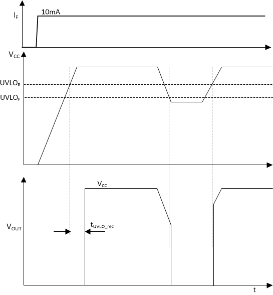
UVLO function is implemented for VCC and VEE pins to prevent an under-driven condition on IGBTs and MOSFETs. When VCC is lower than UVLOR at device start-up or lower than UVLOF after start-up, the voltage-supply UVLO feature holds the effected output low, regardless of the input forward current as shown in Table 8-2. The VCC UVLO protection has a hysteresis feature (UVLOhys). This hysteresis prevents chatter when the power supply produces ground noise which allows the device to permit small drops in bias voltage, which occurs when the device starts switching and operating current consumption increases suddenly.
When VCC drops below UVLOF, a delay, tUVLO_rec occurs on the output when the supply voltage rises above UVLOR again.
 Figure 8-5 UVLO functionality