JAJSHR2B september 2019 – october 2020 UCC23511
PRODUCTION DATA
- 1
- 1 特長
- 2 アプリケーション
- 3 概要
- 4 Revision History
- 5 Pin Configuration and Function
-
6 Specifications
- 6.1 Absolute Maximum Ratings
- 6.2 ESD Ratings
- 6.3 Recommended Operating Conditions
- 6.4 Thermal Information
- 6.5 Power Ratings
- 6.6 Insulation Specifications
- 6.7 Safety-Related Certifications
- 6.8 Safety Limiting Values
- 6.9 Electrical Characteristics
- 6.10 Switching Characteristics
- 6.11 Insulation Characteristics Curves
- 6.12 Typical Characteristics
- 7 Parameter Measurement Information
- 8 Detailed Description
- 9 Application and Implementation
- 10Power Supply Recommendations
- 11Layout
- 12Mechanical, Packaging, and Orderable Information
パッケージ・オプション
デバイスごとのパッケージ図は、PDF版データシートをご参照ください。
メカニカル・データ(パッケージ|ピン)
- DWY|6
サーマルパッド・メカニカル・データ
発注情報
9.2.2.2 Gate Driver Output Resistor
The external gate-driver resistors, RG(ON) and RG(OFF) are used to:
- Limit ringing caused by parasitic inductances and capacitances
- Limit ringing caused by high voltage or high current switching dv/dt, di/dt, and body-diode reverse recovery
- Fine-tune gate drive strength, specifically peak sink and source current to optimize the switching loss
- Reduce electromagnetic interference (EMI)
The output stage of UCC23511 has a pull up structure consisting of a P-channel MOSFET and an N-channel MOSFET in parallel, as shown in Figure 8-4. The N-channel MOSFET provides the peak current that charges the gate of the IGBT (or power switch) while the P-channel MOSFET ensures that VOUT will go all the way upto VCC. Figure 9-1 shows the internal gate resistance, RG_int of the power switch. RG_intis usually specified in the datasheet of the power switch. When turning the power switch "on", the gate driver sees a total gate resistance RG_total = RGON + RG_int and when turning the power switch "off", the gate driver sees a total gate resistance RG_total = RGOFF + RG_int in series with the gate capacitance where,
- RGON is the external resistance on the pcb for turn "on"
- RGOFF is the external resistance on the pcb for turn "off"
- RG_int is the internal gate resistance of the power switch that can be found in the data sheet of the power switch
- Ideal diodes — zero resistance and zero voltage drop — are assumed on both the turn-on and turn-off paths, for simplicity.
To illustrate the procedure to select RGON and RGOFF , let us consider the following example with the assumptions listed below:
- Power switch internal gate resistance is 2 ohms
- Desired charging current is 1.5A
- Desired discharging current is 1.7A
- Gate driver supply is 15 V
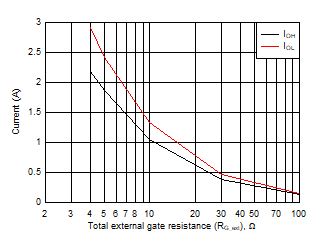
For this example, since VCC=15V, use the typical curves shown in Figure 9-5. It can be seen that we need a total turn on resistance of 7 ohms (peak charging current of 1.5A) and a total turn off resistance of 8 ohms (peak discharging current of 1.7A). Subtracting the internal gate resistance of the power switch, we get RGON= 7 ohms - 2 ohms = 5 ohms, and RGOFF= 8 ohms- 2 ohms = 6 ohms.
 Figure 9-5 Peak drive current vs Total gate resistance, RG_total (Gate driver supply =15V)
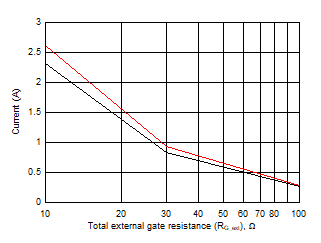
 Figure 9-6 Peak drive current vs Total gate resistance, RG_total (Gate driver supply = 30V)
Use Table 9-3 to find the minimum gate resistance to be used with UCC23511 when driving a power switch. The values shown includes the power switch internal gate resistance RG_int. Hence, RG_int must be subtracted from the values shown to determine the value of the resistor to populate on the printed circuit board.
| Gate driver supply VCC-VEE (V) | Minimum total gate resistance (Ω) = (RGON+ RG_int) or (RGOFF+ RG_int) |
|---|---|
| 15 | 4 |
| 23 | 7 |
| 30 | 10 |
The diodes shown in series with each, RGON and RGOFF, in Figure 9-1 ensure the gate drive current flows through the intended path, respectively, during turn-on and turn-off. Note that the diode forward drop will reduce the voltage level at the gate of the power switch. To achieve rail-to-rail gate voltage levels, add a resistor from the VOUT pin to the power switch gate, with a resistance value approximately 20 times higher than RGON and RGOFF. For the examples described in this section, a good choice is 100 Ω to 200 Ω.
The estimated peak current is also influenced by PCB layout and load capacitance. Parasitic inductance in the gate-driver loop can slow down the peak gate-drive current and introduce overshoot and undershoot. Therefore, TI strongly recommends that the gate-driver loop should be minimized. Conversely, the peak source and sink current is dominated by loop parasitics when the load capacitance (CISS) of the power transistor is very small (typically less than 1 nF) because the rising and falling time is too small and close to the parasitic ringing period.