JAJSKQ6B May 2020 – March 2021 UCC23513-Q1
PRODUCTION DATA
- 1 特長
- 2 アプリケーション
- 3 概要
- 4 Revision History
- 5 Pin Configuration and Function
-
6 Specifications
- 6.1 Absolute Maximum Ratings
- 6.2 ESD Ratings
- 6.3 Recommended Operating Conditions
- 6.4 Thermal Information
- 6.5 Power Ratings
- 6.6 Insulation Specifications
- 6.7 Safety-Related Certifications
- 6.8 Safety Limiting Values
- 6.9 Electrical Characteristics
- 6.10 Switching Characteristics
- 6.11 Insulation Characteristics Curves
- 6.12 Typical Characteristics
- 7 Parameter Measurement Information
- 8 Detailed Description
- 9 Application and Implementation
- 10Power Supply Recommendations
- 11Layout
- 12Mechanical, Packaging, and Orderable Information
8.3.3 Output Stage
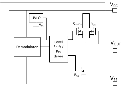
The output stages of the UCC23513-Q1 family feature a pullup structure that delivers the highest peak-source current when it is most needed which is during the Miller plateau region of the power-switch turnon transition (when the power-switch drain or collector voltage experiences dV/dt). The output stage pullup structure features a P-channel MOSFET and an additional pull-up N-channel MOSFET in parallel. The function of the N-channel MOSFET is to provide a brief boost in the peak-sourcing current, enabling fast turnon. Fast turnon is accomplished by briefly turning on the N-channel MOSFET during a narrow instant when the output is changing states from low to high. The on-resistance of this N-channel MOSFET (RNMOS) is approximately 5.1 Ω when activated.
| RNMOS | ROH | ROL | UNIT |
|---|---|---|---|
| 5.1 | 9.5 | 0.40 | Ω |
The ROH parameter is a DC measurement and is representative of the on-resistance of the P-channel device only. This parameter is only for the P-channel device because the pullup N-channel device is held in the OFF state in DC condition and is turned on only for a brief instant when the output is changing states from low to high. Therefore, the effective resistance of the UCC23513-Q1 pullup stage during this brief turnon phase is much lower than what is represented by the ROH parameter, yielding a faster turn on. The turnon-phase output resistance is the parallel combination ROH || RNMOS.
The pulldown structure in the UCC23513-Q1 is simply composed of an N-channel MOSFET. The output voltage swing between VCC and VEE provides rail-to-rail operation because of the MOS-out stage which delivers very low dropout.
 Figure 8-4 Output Stage