SLUSCG0B December 2015 – July 2024 UCC27211A-Q1
PRODUCTION DATA
- 1
- 1 Features
- 2 Applications
- 3 Description
- 4 Pin Configuration and Functions
- 5 Specifications
- 6 Detailed Description
- 7 Application and Implementation
- 8 Power Supply Recommendations
- 9 Layout
- 10Device and Documentation Support
- 11Revision History
- 12Mechanical, Packaging, and Orderable Information
パッケージ・オプション
メカニカル・データ(パッケージ|ピン)
サーマルパッド・メカニカル・データ
- DDA|8
発注情報
3 Description
The UCC27211A-Q1 device driver is based on the popular UCC27201 MOSFET drivers; but, this device offers several significant performance improvements.
The peak output pullup and pulldown current has been increased to 3.7A source and 4.5A sink and thereby allows for driving large power MOSFETs with minimized switching losses during the transition through the Miller Plateau of the MOSFET. The input structure can directly handle –10VDC, which increases robustness and also allows direct interface to gate-drive transformers without using rectification diodes. The inputs are also independent of supply voltage and have a 20V maximum rating.
The switching node of the UCC27211A-Q1 (HS pin) can handle –(24 - VDD) V maximum, which allows the high-side channel to be protected from inherent negative voltages caused by parasitic inductance and stray capacitance. The UCC27211A-Q1 (TTL inputs) has increased hysteresis that allows for interface to analog or digital PWM controllers with enhanced noise immunity.
The low-side and high-side gate drivers are independently controlled and matched to 4ns between the turn on and turn off of each other. An on-chip 120V rated bootstrap diode eliminates the external discrete diodes. Undervoltage lockout is provided for both the high-side and the low-side drivers which provides symmetric turn on and turn off behavior and forces the outputs low if the drive voltage is below the specified threshold.
| PART NUMBER | PACKAGE(1) | BODY SIZE (NOM) |
|---|---|---|
| UCC27211A-Q1 | DDA (PowerPAD™ SOIC, 8) | 4.9mm × 3.9mm |
| D (SOIC, 8) | 4.9mm × 3.9mm |
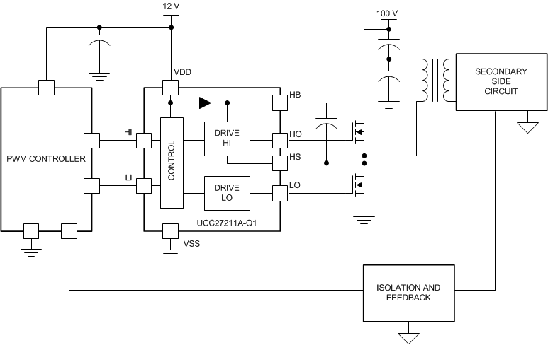
 Typical Application
Diagram
 Propagation Delays vs Supply Voltage T =
25°C