JAJSS81I September   2008  – November 2023 UCC27423-Q1 , UCC27424-Q1 , UCC27425-Q1

PRODUCTION DATA  

  1.   1
  2. 特長
  3. アプリケーション
  4. 概要
  5. Device Comparison Table
  6. Pin Configuration and Functions
  7. Specifications
    1. 6.1 Absolute Maximum Ratings
    2. 6.2 ESD Ratings
    3. 6.3 Recommended Operating Conditions
    4. 6.4 Thermal Information
    5. 6.5 Electrical Characteristics
    6. 6.6 Switching Characteristics
    7. 6.7 Dissipation Ratings
    8. 6.8 Typical Characteristics
  8. Detailed Description
    1. 7.1 Overview
    2. 7.2 Functional Block Diagram
    3. 7.3 Feature Description
      1. 7.3.1 Input Stage
      2. 7.3.2 Output Stage
      3. 7.3.3 Enable
      4. 7.3.4 Parallel Outputs
      5. 7.3.5 Operational Waveforms and Circuit Layout
      6. 7.3.6 VDD
    4. 7.4 Device Functional Modes
  9. Application and Implementation
    1. 8.1 Application Information
    2. 8.2 Typical Application
      1. 8.2.1 Design Requirements
      2. 8.2.2 Detailed Design Procedure
        1. 8.2.2.1 Source and Sink Capabilities During Miller Plateau
        2. 8.2.2.2 Drive Current and Power Requirements
      3. 8.2.3 Application Curves
  10. Power Supply Recommendations
  11. 10Layout
    1. 10.1 Layout Guidelines
    2. 10.2 Layout Example
    3. 10.3 Thermal Considerations
  12. 11Device and Documentation Support
    1. 11.1 Device Support
      1. 11.1.1 サード・パーティ製品に関する免責事項
    2. 11.2 Documentation Support
      1. 11.2.1 Related Documentation
    3. 11.3 ドキュメントの更新通知を受け取る方法
    4. 11.4 サポート・リソース
    5. 11.5 Trademarks
    6. 11.6 静電気放電に関する注意事項
    7. 11.7 用語集
  13. 12Revision History
  14. 13Mechanical, Packaging, and Orderable Information

パッケージ・オプション

メカニカル・データ(パッケージ|ピン)
サーマルパッド・メカニカル・データ
発注情報

Application Curves

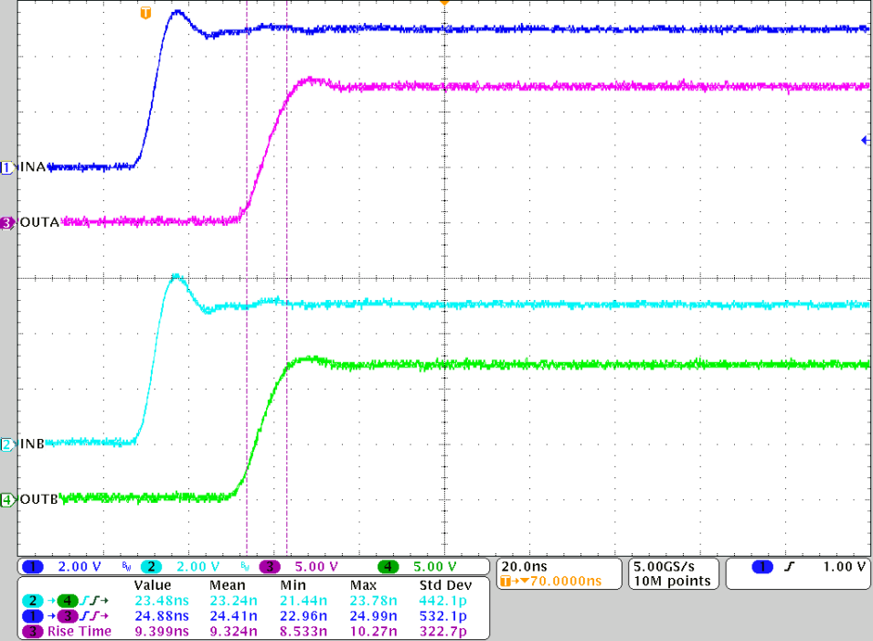
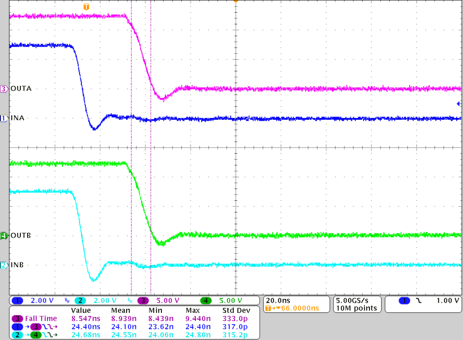
Figure 8-4 and Figure 8-5 show rising and falling time and turnon and turnoff propagation delay testing waveform in room temperature for UCC27424-Q1, and waveform measurement data (see the bottom part of the waveform). Each channel, INA/INB/OUTA/OUTB, is labeled and displayed on the left hand of the waveforms.

The load capacitance testing condition is 1.8 nF, VDD = 12 V, and f = 300 kHz.

HI and LI share one same input from function generator; therefore, besides the propagation delay and rising or falling time, the difference of the propagation delay between HO and LO gives the propagation delay matching data.

Note the linear rise and fall edges of the switching waveforms. This is due to the constant output current characteristic of the driver as opposed to the resistive output impedance of traditional MOSFET-based gate drivers.
GUID-1A586F69-C1D6-43DA-B6A7-7D99B0AEE705-low.png
CL = 1.8 nF, VDD = 12 V, f = 300 kHz
Figure 8-4 Rising Time and Turnon Propagation Delay
GUID-3D393E9D-F10E-4BD4-96F5-B417A7C9ABC2-low.png
CL = 1.8 nF, VDD = 12 V, f = 300 kHz
Figure 8-5 Falling Time and Turnoff Propagation Delay