JAJSS81I September 2008 – November 2023 UCC27423-Q1 , UCC27424-Q1 , UCC27425-Q1
PRODUCTION DATA
- 1
- 1 特長
- 2 アプリケーション
- 3 概要
- 4 Device Comparison Table
- 5 Pin Configuration and Functions
- 6 Specifications
- 7 Detailed Description
- 8 Application and Implementation
- 9 Power Supply Recommendations
- 10Layout
- 11Device and Documentation Support
- 12Revision History
- 13Mechanical, Packaging, and Orderable Information
パッケージ・オプション
メカニカル・データ(パッケージ|ピン)
サーマルパッド・メカニカル・データ
- DGN|8
発注情報
8.2.2.1 Source and Sink Capabilities During Miller Plateau
Large power MOSFETs present a large load to the control circuitry. Proper drive is required for efficient, reliable operation. The UCC2742x-Q1 drivers have been optimized to provide maximum drive to a power MOSFET during the Miller plateau region of the switching transition. This interval occurs while the drain voltage is swinging between the voltage levels dictated by the power topology, requiring the charging and discharging of the drain-gate capacitance with current supplied or removed by the driver device.
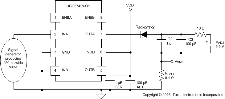
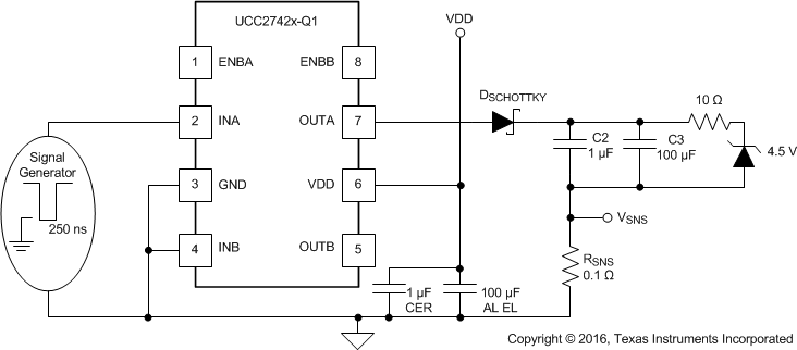
Two circuits are used to test the current capabilities of the UCC2742x-Q1 driver. In each case, external circuitry is added to clamp the output near 5 V while the IC is sinking or sourcing current. An input pulse of 250 ns is applied at a frequency of 1 kHz in the proper polarity for the respective test. In each test, there is a transient period where the current peaked up and then settled down to a steady-state value. The noted current measurements are made at a time of 200 ns after the input pulse is applied, after the initial transient.
The circuit in Figure 8-2 is used to verify the current sink capability when the output of the driver is clamped around 5 V, a typical value of gate-source voltage during the Miller plateau region. The UCC2742x-Q1 is found to sink 4.5 A at VDD = 15 V and 4.28 A at VDD = 12 V.
 Figure 8-2 Current Sink Capability Test
The circuit show in Figure 8-3 is used to test the current source capability with the output clamped around 5 V with a string of Zener diodes. The UCC2742x-Q1 is found to source 4.8 A at VDD = 15 V and 3.7 A at VDD = 12 V.
 Figure 8-3 Current Source Capability Test