JAJSS81I September 2008 – November 2023 UCC27423-Q1 , UCC27424-Q1 , UCC27425-Q1
PRODUCTION DATA
- 1
- 1 特長
- 2 アプリケーション
- 3 概要
- 4 Device Comparison Table
- 5 Pin Configuration and Functions
- 6 Specifications
- 7 Detailed Description
- 8 Application and Implementation
- 9 Power Supply Recommendations
- 10Layout
- 11Device and Documentation Support
- 12Revision History
- 13Mechanical, Packaging, and Orderable Information
パッケージ・オプション
メカニカル・データ(パッケージ|ピン)
サーマルパッド・メカニカル・データ
- DGN|8
発注情報
6.6 Switching Characteristics
over operating free-air temperature range (unless otherwise noted)
| PARAMETER | TEST CONDITIONS | MIN | TYP | MAX | UNIT | ||
|---|---|---|---|---|---|---|---|
| SWITCHING TIME | |||||||
| tr | Rise time (OUTA, OUTB) | CLOAD = 1.8 nF(1) | 20 | 40 | ns | ||
| tf | Fall time (OUTA, OUTB) | CLOAD = 1.8 nF(1) | 15 | 40 | ns | ||
| tD1 | Delay time, IN rising (IN to OUT) | CLOAD = 1.8 nF(1) | 25 | 50 | ns | ||
| tD2 | Delay time, IN falling (IN to OUT) | CLOAD = 1.8 nF(1) | UCC27423-Q1, UCC27424-Q1 | 35 | 60 | ns | |
| UCC27425-Q1 | 35 | 70 | |||||
| ENABLE (ENBA, ENBB) | |||||||
| tD3 | Propagation delay time(3) | CLOAD = 1.8 nF(1)(2) | 30 | 60 | ns | ||
| tD4 | Propagation delay time(3) | CLOAD = 1.8 nF(1)(2) | 100 | 150 | ns | ||
(1) Specified by design
(2) Not production tested
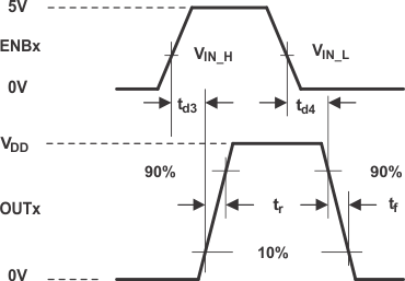
(3) See Figure 6-2

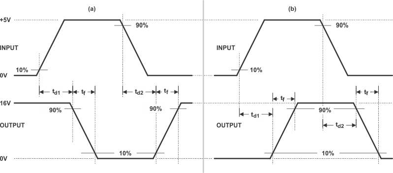
The 10% and 90%
thresholds depict the dynamics of the bipolar output devices that dominate the
power MOSFET transition through the Miller regions of operation.
Figure 6-1 Switching
Waveforms for (a) Inverting Driver and (b) Noninverting Driver
The 10% and 90%
thresholds depict the dynamics of the bipolar output devices that dominate the
power MOSFET transition through the Miller regions of operation.
Figure 6-2 Switching
Waveform for Enable to Output