JAJSC57F November 2002 – November 2023 UCC27423 , UCC27424 , UCC27425
PRODUCTION DATA
- 1
- 1 特長
- 2 アプリケーション
- 3 概要
- 4 Device Comparison Table
- 5 Pin Configuration and Functions
- 6 Specifications
- 7 Detailed Description
- 8 Application and Implementation
- 9 Power Supply Recommendations
- 10Layout
- 11Device and Documentation Support
- 12Revision History
- 13Mechanical, Packaging, and Orderable Information
パッケージ・オプション
デバイスごとのパッケージ図は、PDF版データシートをご参照ください。
メカニカル・データ(パッケージ|ピン)
- D|8
- P|8
- DGN|8
サーマルパッド・メカニカル・データ
- DGN|8
発注情報
6.6 Dissipation Ratings
| PACKAGE | SUFFIX | POWER RATING (mW) TA = 70°C(1) | DERATING FACTOR ABOVE 70°C (mW/°C)(1) |
|---|---|---|---|
| SOIC-8 | D | 344–655(2) | 6.25–11.9(2) |
| PDIP-8 | P | 500 | 9 |
| MSOP(3) | DGN | 1370 | 17.1 |
(1) 125°C operating junction temperature is used for power rating calculations
(2) The range of values indicates the effect of pc-board. These values are intended to give the system designer an indication of the best and worst case conditions. In general, the system designer should attempt to use larger traces on the pc-board where possible in order to spread the heat away form the device more effectively. For information on the PowerPAD™ package, refer to Technical Brief, PowerPad Thermally Enhanced Package, Texas Instruments (SLMA002) and Application Brief, PowerPad Made Easy, Texas Instruments (SLMA004).
(3) The PowerPAD™ is not directly connected to any leads of this package. However, it is electrically and thermally connected to the substrate which is the ground of the device.
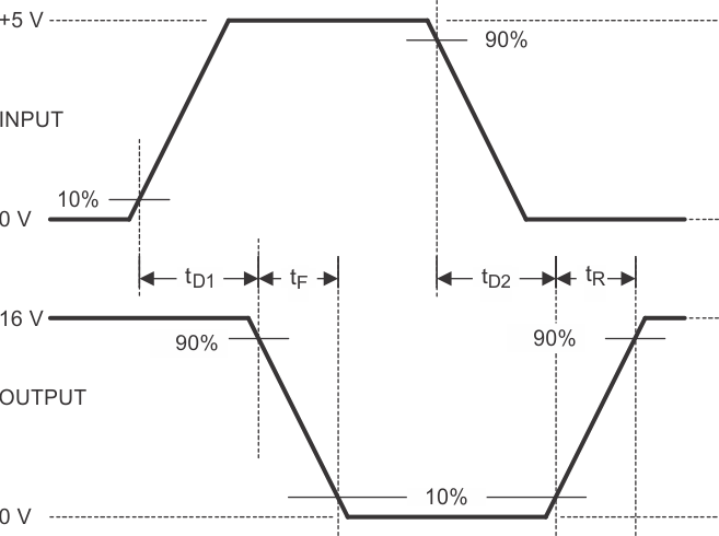
 Figure 6-1 Inverting Driver Switching
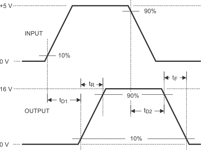
 Figure 6-2 Noninverting Driver Switching
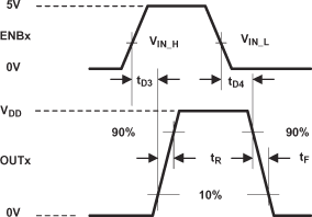
The 10% and 90% thresholds depict the dynamics of the BiPolar output devices that dominate the power MOSFET transition through the Miller regions of operation.
Figure 6-3 Switching Waveform for Enable to Output