SLUSB33A May   2012  – December 2014 UCC27518 , UCC27519

PRODUCTION DATA.  

  1. Features
  2. Applications
  3. Description
  4. Revision History
  5. Description (continued)
  6. Device Comparison Table
  7. Pin Configuration and Functions
  8. Specifications
    1. 8.1 Absolute Maximum Ratings
    2. 8.2 ESD Ratings
    3. 8.3 Recommended Operating Conditions
    4. 8.4 Thermal Information
    5. 8.5 Electrical Characteristics
    6. 8.6 Switching Characteristics
    7. 8.7 Typical Characteristics
  9. Detailed Description
    1. 9.1 Overview
    2. 9.2 Functional Block Diagrams
    3. 9.3 Feature Description
      1. 9.3.1 VDD and Undervoltage Lockout
      2. 9.3.2 Operating Supply Current
      3. 9.3.3 Input Stage
      4. 9.3.4 Enable Function
      5. 9.3.5 Output Stage
      6. 9.3.6 Low Propagation Delays
    4. 9.4 Device Functional Modes
  10. 10Application and Implementation
    1. 10.1 Application Information
    2. 10.2 Typical Application
      1. 10.2.1 Design Requirements
      2. 10.2.2 Detailed Design Procedure
        1. 10.2.2.1 Input-to-Output Logic
        2. 10.2.2.2 Input Threshold Type
        3. 10.2.2.3 VDD Bias Supply Voltage
        4. 10.2.2.4 Peak Source and Sink Currents
        5. 10.2.2.5 Enable and Disable Function
        6. 10.2.2.6 Propagation Delay
      3. 10.2.3 Application Curve
  11. 11Power Supply Recommendations
  12. 12Layout
    1. 12.1 Layout Guidelines
    2. 12.2 Layout Example
    3. 12.3 Thermal Considerations
    4. 12.4 Power Dissipation
  13. 13Device and Documentation Support
    1. 13.1 Related Links
    2. 13.2 Trademarks
    3. 13.3 Electrostatic Discharge Caution
    4. 13.4 Glossary
  14. 14Mechanical, Packaging, and Orderable Information

パッケージ・オプション

メカニカル・データ(パッケージ|ピン)
サーマルパッド・メカニカル・データ
発注情報

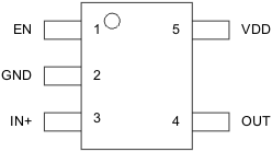
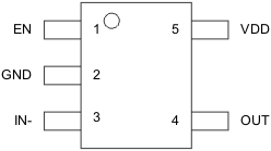
7 Pin Configuration and Functions

UCC27518
SOT-23 DBV
(Top View)
pin2_lusb33.gif
UCC27519
SOT-23 DBV
(Top View)
pin_lusb33.gif

Pin Functions

PIN I/O DESCRIPTION
NO. NAME
1 EN I Enable input: (EN biased LOW disables output regardless of Input state, EN biased high or floating enables output, EN is allowed to float hence it is pin-to-pin compatible with TPS282X N/C pin)
2 GND Ground: All signals referenced to this pin
3 IN– I Input: Inverting input in the UCC27518, output held LOW if IN– is unbiased or floating
IN+ I Input: Noninverting input in the UCC27519, output held LOW if IN+ is unbiased or floating
4 OUT O Sourcing and sinking current output of driver
5 VDD I Supply input