JAJST72A April 2024 – October 2024 UCC27614-Q1
PRODUCTION DATA
- 1
- 1 特長
- 2 アプリケーション
- 3 概要
- 4 Pin Configuration and Functions
- 5 Specifications
- 6 Detailed Description
- 7 Applications and Implementation
- 8 Power Supply Recommendations
- 9 Layout
- 10Device and Documentation Support
- 11Revision History
- 12Mechanical, Packaging, and Orderable Information
パッケージ・オプション
デバイスごとのパッケージ図は、PDF版データシートをご参照ください。
メカニカル・データ(パッケージ|ピン)
- DSG|8
サーマルパッド・メカニカル・データ
- DSG|8
発注情報
6.3.1 VDD Undervoltage Lockout
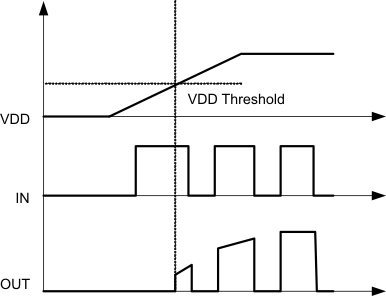
The UCC27614-Q1 device offers an undervoltage lockout threshold of 4 V. The device's hysteresis range helps to avoid any chattering due to the presence of noise on the bias supply. 0.3 V of typical UVLO hysteresis is expected for 4-V UVLO devices. There is no significant driver output turnon delay due to the UVLO feature, and 5 μs of UVLO delay is expected. The UVLO turn-off delay is also minimized as much as possible. The UVLO delay is designed to minimize chattering that may occur due to very fast transients that may appear on VDD. When the bias supply is below UVLO thresholds, the outputs are held actively low irrespective of the state of input pins and enable pin. The device accepts a wide range of slew rates on its VDD pin, and VDD noise within the hysteresis range does not affect the output state of the driver (neither ON nor OFF).
 Figure 6-3 Power Up