JAJSNN4B March 2022 – November 2022 UCC27624-Q1
PRODUCTION DATA
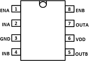
5 Pin Configuration and Functions
 Figure 5-1 D
Package8-Pin SOICTop View
Figure 5-2 DGN Package8-Pin VSSOPTop View
Table 5-1 Pin Functions
| PIN | TYPE(1) | DESCRIPTION | ||
|---|---|---|---|---|
| NAME | DGN | D | ||
| ENA | 1 | 1 | I | Enable input for Channel A. Biasing ENA, LOW will disable Channel A output regardless of the state of INA. Pulling ENA, HIGH enables the Channel A output. If ENA is left floating, Channel A is enabled by default due to an internal pullup resistor. It is recommended to connect this pin to VDD if unused. |
| ENB | 8 | 8 | I | Enable input for Channel B. Biasing ENB, LOW disables Channel B output regardless of the state of INB. Pulling ENB, HIGH enables the Channel B output. If ENB is left floating, Channel B is enabled by default due to an internal pullup resistor. It is recommended to connect this pin to VDD if unused. |
| GND | 3 | 3 | — | Ground: All signals are referenced to this pin. |
| INA | 2 | 2 | I | Input to Channel A. INA is the non-inverting input of the UCC27624-Q1 device. OUTA is held LOW if INA is unbiased or floating by default due to an internal pulldown resistor. Connect this pin to GND if unused. |
| INB | 4 | 4 | I | Input to Channel B. INB is the non-inverting input of the UCC27624-Q1 device. OUTB is held LOW if INB is unbiased or floating by default due to an internal pulldown resistor. Connect this pin to GND if unused. |
| OUTA | 7 | 7 | O | Channel A Output |
| OUTB | 5 | 5 | O | Channel B Output |
| VDD | 6 | 6 | I | Bias supply input. Bypass this pin with two ceramic capacitors, generally ≥ 1 μF and 0.1 μF, which are referenced to GND pin of this device. |
| Thermal Pad | — | — | Connect to GND through large copper plane. This pad is not a low-impedance path to GND. | |
(1) I =
Input; O = Output