SLUSAO7C September 2011 – July 2024 UCC28063
PRODUCTION DATA
- 1
- 1 Features
- 2 Applications
- 3 Description
- 4 Revision History
- 5 Pin Configuration and Functions
- 6 Specifications
-
7 Detailed Description
- 7.1 Overview
- 7.2 Functional Block Diagram
- 7.3
Feature Description
- 7.3.1 Principles of Operation
- 7.3.2 Natural Interleaving
- 7.3.3 On-Time Control, Maximum Frequency Limiting, and Restart Timer
- 7.3.4 Distortion Reduction
- 7.3.5 Zero-Current Detection and Valley Switching
- 7.3.6 Phase Management and Light-Load Operation
- 7.3.7 External Disable
- 7.3.8 Improved Error Amplifier
- 7.3.9 Soft Start
- 7.3.10 Brownout Protection
- 7.3.11 Dropout Detection
- 7.3.12 VREF
- 7.3.13 VCC
- 7.3.14 Control of Downstream Converter
- 7.3.15
System Level Protections
- 7.3.15.1 Failsafe OVP - Output Overvoltage Protection
- 7.3.15.2 Overcurrent Protection
- 7.3.15.3 Open-Loop Protection
- 7.3.15.4 VCC Undervoltage Lock-Out (UVLO) Protection
- 7.3.15.5 Phase-Fail Protection
- 7.3.15.6 CS-Open, TSET-Open and -Short Protection
- 7.3.15.7 Thermal Shutdown Protection
- 7.3.15.8 AC-Line Brownout and Dropout Protections
- 7.3.15.9 Fault Logic Diagram
- 7.4 Device Functional Modes
-
8 Applications and Implementation
- 8.1 Application Information
- 8.2
Typical Application
- 8.2.1 Design Requirements
- 8.2.2
Detailed Design Procedure
- 8.2.2.1 Inductor Selection
- 8.2.2.2 ZCD Resistor Selection (RZA, RZB)
- 8.2.2.3 HVSEN
- 8.2.2.4 Output Capacitor Selection
- 8.2.2.5 Selecting (RS) For Peak Current Limiting
- 8.2.2.6 Power Semiconductor Selection (Q1, Q2, D1, D2)
- 8.2.2.7 Brownout Protection
- 8.2.2.8 Converter Timing
- 8.2.2.9 Programming VOUT
- 8.2.2.10 Voltage Loop Compensation
- 8.2.3 Application Curves
- 9 Power Supply Recommendations
- 10Layout
- 11Device and Documentation Support
- 12Mechanical, Packaging, and Orderable Information
パッケージ・オプション
メカニカル・データ(パッケージ|ピン)
- D|16
サーマルパッド・メカニカル・データ
- D|16
発注情報
7.3.1 Principles of Operation
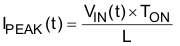
The UCC28063 contains the control circuits for two parallel-connected boost pulse-width modulated (PWM) power converters. The boost PWM power converters ramp current in the boost inductors for a time period proportional to the voltage on the error amplifier output. Each power converter then turns off the power MOSFET until current in the boost inductor decays to zero, as sensed on the zero current detection inputs (ZCDA and ZCDB). Once the inductor is demagnetized, the power converter starts another cycle. This on/off cycling produces a triangle wave of current, with peak current set by the on-time and instantaneous power mains input voltage, VIN(t), as shown in Equation 1.
The average line current is exactly equal to half of the peak line current, as shown in Equation 2.
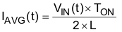
With TON and L being essentially constant during an AC-line period, the resulting triangular current waveform during each switching cycle will have an average value proportional to the instantaneous value of the rectified AC-line voltage. This architecture results in a resistive input impedance characteristic at the line frequency and a near-unity power factor.