SNVSA88C December 2014 – November 2016 UCC28063A
PRODUCTION DATA.
- 1 Features
- 2 Applications
- 3 Description
- 4 Revision History
- 5 Description (Continued)
- 6 Pin Configuration and Functions
- 7 Specifications
-
8 Detailed Description
- 8.1 Overview
- 8.2 Functional Block Diagram
- 8.3
Feature Description
- 8.3.1 Principles of Operation
- 8.3.2 Natural Interleaving
- 8.3.3 On-Time Control, Maximum Frequency Limiting, and Restart Timer
- 8.3.4 Distortion Reduction
- 8.3.5 Zero-Current Detection and Valley Switching
- 8.3.6 Phase Management and Light-Load Operation
- 8.3.7 External Disable
- 8.3.8 Improved Error Amplifier
- 8.3.9 Soft Start
- 8.3.10 Brownout Protection
- 8.3.11 Dropout Detection
- 8.3.12 VREF
- 8.3.13 VCC
- 8.3.14 Control of Downstream Converter
- 8.3.15
System Level Protections
- 8.3.15.1 Failsafe OVP - Output Overvoltage Protection
- 8.3.15.2 Overcurrent Protection
- 8.3.15.3 Open-Loop Protection
- 8.3.15.4 VCC Undervoltage Lock-Out (UVLO) Protection
- 8.3.15.5 Phase-Fail Protection
- 8.3.15.6 Thermal Shutdown Protection
- 8.3.15.7 AC-Line Brownout and Dropout Protections
- 8.3.15.8 Fault Logic Diagram
- 8.4 Device Functional Modes
-
9 Applications and Implementation
- 9.1 Application Information
- 9.2
Typical Application
- 9.2.1 Design Requirements
- 9.2.2
Detailed Design Procedure
- 9.2.2.1 Inductor Selection
- 9.2.2.2 ZCD Resistor Selection (RZA, RZB)
- 9.2.2.3 HVSEN
- 9.2.2.4 Output Capacitor Selection
- 9.2.2.5 Selecting (RS) For Peak Current Limiting
- 9.2.2.6 Power Semiconductor Selection (Q1, Q2, D1, D2)
- 9.2.2.7 Brownout Protection
- 9.2.2.8 Converter Timing
- 9.2.2.9 Programming VOUT
- 9.2.2.10 Voltage Loop Compensation
- 9.2.3 Application Curves
- 10Power Supply Recommendations
- 11Layout
- 12Device and Documentation Support
- 13Mechanical, Packaging, and Orderable Information
8 Detailed Description
8.1 Overview
This part is identical to UCC28063 with the exception that the TSET pin Open/ Short Fault Detect and the CS pin Open Fault Detect features are removed. Removal of these fault detect mechanisms provides a higher degree of noise immunity for applications where significant voltage noise could be coupled onto the TSET or CS pins during conditions of extreme fast transient, surge or impulse noise events. The Soft Re-Start fault protection which would be triggered on the UCC28063 will not occur with the UCC28063A. The system will continue to provide power delivery through such events, albeit with the possibility of some dynamic regulation irregularity.
Transition Mode Control is the most popular choice for the Boost Power Factor Correction topology at lower power levels because of its lower complexity in achieving high power factor while at the same time not placing demanding requirements on the power component specifications. A lower cost boost diode with higher reverse recovery current specification may be used, for instance, in the Transition Mode Boost. Interleaved Transition Mode Control retains this benefit and generally extends the applicability up to much higher power levels while simultaneously conferring the interleaving benefits of reduced input and output ripple, phase management for light load efficiency enhancement, redundancy, system thermal optimization and low profile or planar solutions.
The UCC28063A enables a very cost effective solution with a particular focus on ruggedness, fault management, fault recovery, efficiency and higher end performance in areas such as acoustic management and fast transient response. It may be regarded as an enhanced and new generation UCC28061.
Interleaving control and phase management facilitates 80+ and Energy Star designs with reduced input and output ripple. The Natural Interleaving method allows TM operation and achieves 180 degrees between the phases by On-time management and does not rely on tight tolerance requirements on the inductors. The Crossover Notch Reduction block implements a non-linear current shaping characteristic on the instantaneous voltage sense (VINAC) in order to reduce distortion and increase Power Factor. Negative current sensing is implemented on the total input current instead of just the MOSFET current which prevents MOSFET switching during inrush surges or in any mode where the inductor current may become substantially continuous (CCM). This prevents reverse recovery conduction events between the MOSFET and output rectifier. Downstream power stage management is facilitated by the PWMCNTL signal. This open drain signal provides an enable with hysteresis for a downstream converter when the PFC stage voltage is above an operating threshold, FailSafe OV protection is not in operation and there is no PhaseFail fault.
Independent output voltage sense chains with their separate fault management behaviors provide a high degree of redundancy against PFC stage overvoltage. Brown-Out, HVSENSE OV, UVLO, and IC Overtemperature will all cause a complete Soft-Start cycle. Other faults such as short duration AC Drop-Out, minor overvoltage or cycle-by-cycle overcurrent cause a live recovery process to initiate by pulling down on the COMP pin or by terminating the pulses early.
In general IC operation is designed to ensure smooth and acoustic noise free start-up, good transient response behavior and well behaved recovery from faults. The Error amplifier transconductance is designed to allow smaller compensation components and optimum transient response for larger deviations. The Soft-Start process is carefully optimized. A complete Soft Start is implemented on recovery from every fault, for consistency. The Soft Start speed is dependent on the output voltage sense to speed up start-up from low AC line and to minimize the effect of excessive "COMP" during start-up into no-load. This complete discharge of COMP aids with preventing excessive currents on recovery from an AC Brown-Out event.
8.2 Functional Block Diagram
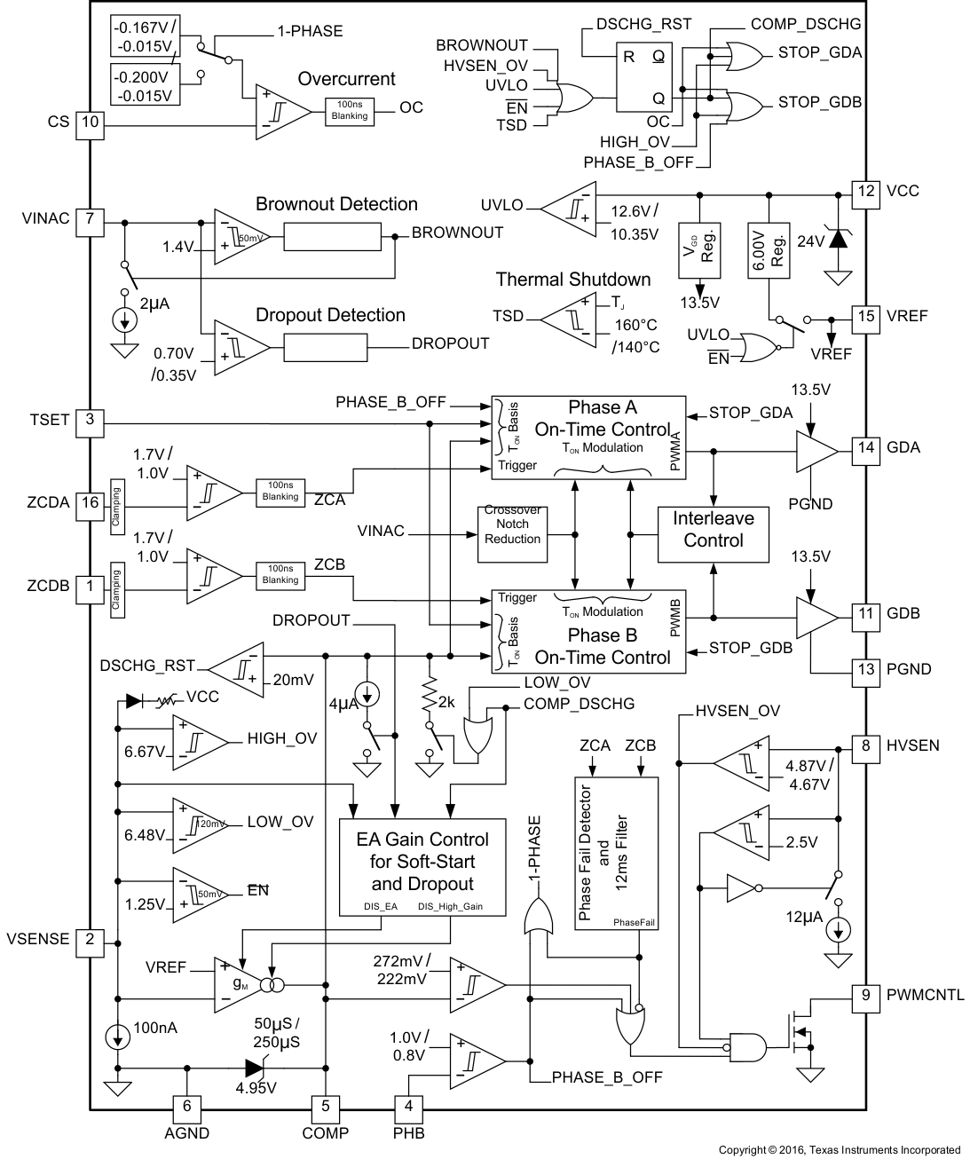
8.3 Feature Description
8.3.1 Principles of Operation
The UCC28063A contains the control circuits for two parallel-connected boost pulse-width modulated (PWM) power converters. The boost PWM power converters ramp current in the boost inductors for a time period proportional to the voltage on the error amplifier output. Each power converter then turns off the power MOSFET until current in the boost inductor decays to zero, as sensed on the zero current detection inputs (ZCDA and ZCDB). Once the inductor is demagnetized, the power converter starts another cycle. This on/off cycling produces a triangle wave of current, with peak current set by the on-time and instantaneous power mains input voltage, VIN(t), as shown in Equation 1.

The average line current is exactly equal to half of the peak line current, as shown in Equation 2.

With TON and L being essentially constant during an AC-line period, the resulting triangular current waveform during each switching cycle will have an average value proportional to the instantaneous value of the rectified AC-line voltage. This architecture results in a resistive input impedance characteristic at the line frequency and a near-unity power factor.
8.3.2 Natural Interleaving
Under normal operating conditions, the UCC28063A regulates the relative phasing of the channel A and channel B inductor currents to be very close to 180°. This greatly reduces the switching-frequency ripple currents seen at the line-filter and output capacitors, compared to the ripple current of each individual converter. This design allows a reduction in the size and cost of input and output filtering. The phase-control function differentially modulates the on-times of the A and B channels based on their phase and frequency relationship. The Natural Interleaving method allows the converter to achieve 180° phase-shift and transition-mode operation for both phases without tight requirements on boost inductor tolerance.
Ideally, the best current-sharing is achieved when both inductors are exactly the same value. Typically the inductances are not the same, so the current-sharing of the A and B channels is proportional to the inductor tolerance. Also, switching delays and resonances of each channel typically differ slightly, and the controller allows some necessary phase-error deviation from 180° to maintain equal switching frequencies. Optimal phase balance occurs if the individual power stages and the on-times are well matched. Mismatches in inductor values do not affect the phase relationship.
8.3.3 On-Time Control, Maximum Frequency Limiting, and Restart Timer
Gate-drive on-time varies proportionately with the error-amplifier output voltage by a factor called KT (in units of μs/V), as shown in Equation 3.

Where:
- VCOMP is the output voltage of the error amplifier and 125 mV is a modulator offset voltage.
The maximum output of the error amplifier is limited to 4.95 V. This value, minus the 125-mV modulator offset, limits maximum on-time as determined by Equation 4.

This on-time limit sets the maximum power that can be delivered by the converter at a given input voltage.
At lower power, one boost channel (phase) may be turned off to achieve efficiency benefits (see Phase Management section, below). To provide a smooth transition between two-phase and single-phase operation, KT increases by a factor of two in single-phase mode:

The maximum switching frequency of each phase is limited by minimum-period timers. If inductor current decays to zero before the minimum-period timer elapses, the next turn-on will be delayed, resulting in discontinuous phase current.
A restart timer ensures starting under all circumstances by restarting both phases if the ZCD input of either phase has not transitioned from high-to-low within approximately 200 µs. To prevent the circuit from operating in continuous conduction mode (CCM), the restart timer does not trigger turn-on until both phase-currents return to zero.
The on-time factors (KT, KTS) and the minimum switching period, T(MIN), are proportional to the time-setting resistor RTSET (the resistor from the TSET pin to ground), and these factors can be calculated by Equation 5, Equation 6 and Equation 7:


The proper value of RTSET will result in the clamped maximum on-time, TON(max), required by the converter operating at the minimum input line voltage and maximum load.
8.3.4 Distortion Reduction
Due to the parasitic resonance between the drain-source capacitance of the switching MOSFET and the boost inductor, conventional transition-mode PFC circuits may not be able to absorb power from the input line when the input voltage is near zero. This limitation increases total harmonic distortion as a result of ac-line current waveform distortion in the form of flat spots. To help reduce line-current distortion, the UCC28063A increases switching MOSFET on-time when the input voltage is near 0 V to improve the power absorption capability and compensate for this effect.
Figure 12 in the Typical Characteristics section shows the increase in on-time with respect to VINAC voltage. Excessive filtering of the VINAC signal will nullify this function.
8.3.5 Zero-Current Detection and Valley Switching
In transition-mode PFC circuits, the MOSFET turns on when the boost inductor current reaches zero. Because of the resonance between the boost inductor and the parasitic capacitance at the MOSFET drain node, part of the energy stored in the MOSFET junction capacitor can be recovered, reducing switching losses. Furthermore, when the rectified input voltage is less than half of the output voltage, all the energy stored in the MOSFET junction capacitor can be recovered and zero-voltage switching (ZVS) can be realized. By adding an appropriate delay, the MOSFET can be turned on at the valley of its resonating drain voltage (valley-switching). In this way, the energy recovery can be maximized and switching loss is minimized.
The optimal time delay is generally derived empirically, but a good starting point is a value equal to 25% of the resonant period of the drain circuit. The delay can be realized by a simple RC filter, as shown in Figure 25, but the delay time increases slightly as the input voltage nears the output voltage. Because the ZCD pin is internally clamped, a more accurate delay can also be realized by using the circuit shown in Figure 26.
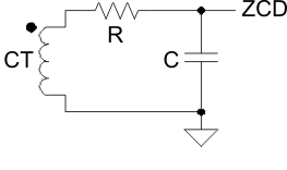 Figure 25. Simple RC Delay Circuit
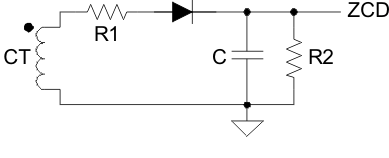 Figure 26. More Accurate Time Delay Circuit
8.3.6 Phase Management and Light-Load Operation
Under light-load conditions, switching losses may dominate over conduction losses and efficiency may be improved if one phase (channel) is turned off. At a certain power level, the reduction of switching losses is greater than the increase in conduction losses. Turning off one phase at light load is especially valuable for meeting light-load efficiency standards. This is one of the major benefits of interleaved PFC and it is especially valuable for meeting 80+ design requirements.
The PHB input can be used to force the UCC28063A to operate in single-phase mode. When PHB is driven below 0.8 V, channel B will stop switching and channel A on-time will automatically double to compensate. The device will resume dual-phase mode when PHB is raised above 1.0 V. For customized phase management, an external circuit can detect the conditions for switching to single-phase operation and drive PHB accordingly. To operate continuously in two-phase mode (normal mode) when phase management is not desired, simply connect PHB to VREF.
As load current decreases, the error amplifier commands less ac-line input current by lowering COMP voltage. In applications where the ac-line is limited to the low-voltage range only, it may be advantageous to connect PHB directly to COMP to allow automatic selection of single-phase operation without additional external circuitry.
8.3.7 External Disable
The UCC28063A can be externally disabled by purposefully grounding the VSENSE pin with an open-drain or open-collector driver. When disabled, the device supply current drops significantly and COMP is actively pulled low. This disable method forces the device into standby mode and minimizes its power consumption. This is particularly useful when standby power is a key design aspect. When VSENSE is released, the device enters soft-start mode.
8.3.8 Improved Error Amplifier
The voltage-error amplifier is a transconductance amplifier. Voltage-loop compensation is connected from the error amplifier output, COMP, to analog ground, AGND. The recommended Type-II compensation network is shown in Figure 27. For loop-stability purposes, the compensation network values are calculated based on small-signal perturbations of the output voltage using the nominal transconductance (gain) of 55 μS.
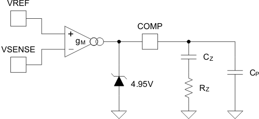 Figure 27. Transconductance Error Amplifier With Typical Compensation Network
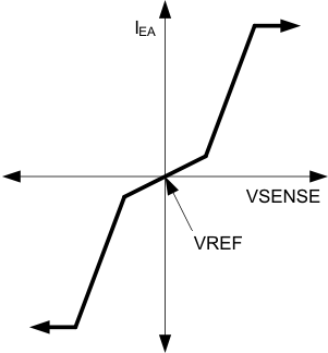
To improve the transient response to large perturbations, the error amplifier gain increases by a factor of ~5X when the error amp input deviates more than ±5% from the nominal regulation voltage, VSENSEreg. This increase allows faster charging and discharging of the compensation components following sudden load-current increases or decreases (also refer to Figure 5 in the Typical Characteristics).
8.3.9 Soft Start
Soft-start is a process for boosting the output voltage of the PFC converter from the peak of the ac-line input voltage to the desired regulation voltage under controlled conditions. Instead of a dedicated soft-start pin, the UCC28063A uses the voltage error amplifier as a controlled current source to increase the PWM duty-cycle by way of increasing the COMP voltage. To avoid excessive start-up time-delay when the ac-line voltage is low, a higher current is applied until VSENSE exceeds 3 V at which point the current is reduced to minimize the tendency for excess COMP voltage at no-load start-up.
The PWM gradually ramps from zero on-time to normal on-time as the compensation capacitor from COMP to AGND charges from zero to near its final value. This process implements a soft-start, with timing set by the output current of the error amplifier and the value of the compensation capacitors. In the event of a HVSEN FailSafe OVP, brownout, external-disable, UVLO fault, or other protection faults, COMP is actively discharged and the UCC28063A will soft-start after the triggering event is cleared. Even if a fault event happens very briefly, the fault is latched into the soft-start state and soft-start is delayed until COMP is fully discharged to 20 mV and the fault is cleared. See Figure 29 for details on the COMP current. See Figure 30 which illustrates an example of typical system behavior during soft-start.
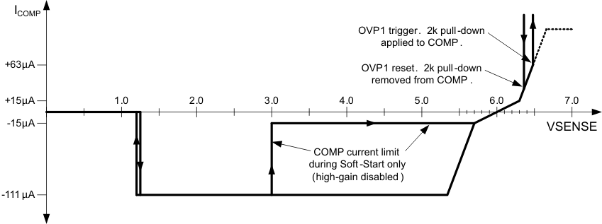
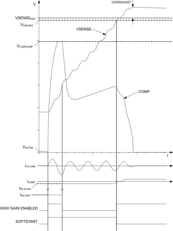 Figure 30. Soft-Start Timing With Illustrative System Behavior
8.3.10 Brownout Protection
As the power line RMS voltage decreases, RMS input current must increase to maintain a constant output voltage for a specific load. Brownout protection helps prevent excess system thermal stress (due to the higher RMS input current) from exceeding a safe operating level. Power-line voltage is sensed at VINAC. When the VINAC fails to exceed the brownout threshold for the brownout filter time, a brownout condition is detected and both gate drive outputs are turned off. During brownout, COMP is actively pulled low and a soft-start condition is initiated. Hysteresis is built into the brownout detection circuit to avoid chatter around the threshold. When VINAC rises above the brownout threshold, the power stage soft-starts as COMP rises with controlled current.
The brownout detection threshold and its hysteresis are set by the voltage-divider ratio and resistor values. Brownout protection is based on VINAC peak voltage; the threshold and hysteresis are also based on the line peak voltage. Major hysteresis is provided by a 2-μA current-sink (IBOHYS) enabled whenever VINAC falls below the brownout detection threshold. Minor hysteresis is also present in the form of a 50-mV offset (VBOHYS) between the VINAC detection and clear thresholds. The peak VINAC voltage can be easily translated into an RMS value. Example resistor values for the voltage divider are 8.61 MΩ ±1% from the rectified input voltage to VINAC and 133 kΩ ±1% from VINAC to ground. These resistors set the typical thresholds for RMS line voltages, as shown in Table 1.
Table 1. Brownout Thresholds (For Conditions Stated in the Text)
| THRESHOLD | AC-LINE VOLTAGE (RMS) |
|---|---|
| Falling | 66 V |
| Rising | 78 V |
Equation 8 and Equation 9 can be used to calculate the VINAC divider-resistor values based on desired brownout detection and brownout clear voltage levels. VAC_OK is the desired RMS turn-on voltage, VAC_BO is the desired RMS turn-off brownout voltage, and VLOSS is total series voltage drop due to wiring, EMI-filter, and bridge-rectifier impedances at VAC_BO. VBODET, VBOHYS and IBOHYS are found in the data-tables of this datasheet.


Once standard values for the VINAC divider-resistors RA and RB are selected, the actual turn-on and brownout threshold RMS voltages for the ac-line can be back-calculated with Equation 10 and Equation 11:


An example of the timing for the brownout function is illustrated in Figure 31.
For a quick estimation of the turn-on and brownout voltages, simplify the foregoing equations by setting the VLOSS and VBOHYS terms to zero.
8.3.11 Dropout Detection
It is often the case that the ac-line voltage momentarily drops to zero or nearly zero, due to transient abnormal events affecting the local ac power distribution network. Referred to as ac-line dropouts (or sometimes as line-dips) the duration of such events usually extends to only 1 or 2 line cycles. During a dropout, the down-stream power conversion stages depend on sufficient energy storage in the PFC output capacitance, which is sized to provide the ride-through energy for a specified hold-up time. Typically while the PFC output voltage is falling, the voltage-loop error amplifier output rises in an attempt to maintain regulation. As a consequence, excess duty-cycle is commanded when the ac-line voltage returns and high peak current surges may saturate the boost inductors with possible overstress and audible noise.
The UCC28063A incorporates a dropout detection feature which suspends the action of the error amplifier for the duration of the dropout. If the VINAC voltage falls below 0.35 V for longer than 5 ms, a dropout condition is detected and the error amplifier output is turned off. In addition, a 4-μA pull-down current is applied to COMP to gently discharge the compensation network capacitors. In this way, when the ac-line voltage returns, the COMP voltage (and corresponding duty-cycle setting) remains very near or even slightly below the level it was before the dropout occurred. Current surges due to excess duty-cycle, and their undesired attendant effects, are avoided. The dropout condition is cancelled and the error amplifier resumes normal operation when VINAC rises above 0.71 V.
Based on the VINAC divider-resistor values calculated for brownout in the previous section, the input RMS voltage thresholds for dropout detection VAC_DO and dropout clearing VDO_CLR can be determined using Equation 12 and Equation 13, below.


Avoid excessive filtering of the VINAC signal, or dropout detection may be delayed or defeated. An RC time-constant of ≤ 100-μs should provide good performance. An example of the timing for the dropout function is illustrated in Figure 32.
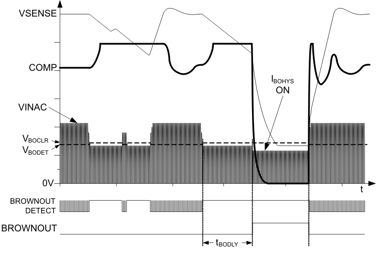 Figure 31. AC-Line Brownout Timing With Illustrative System Behavior
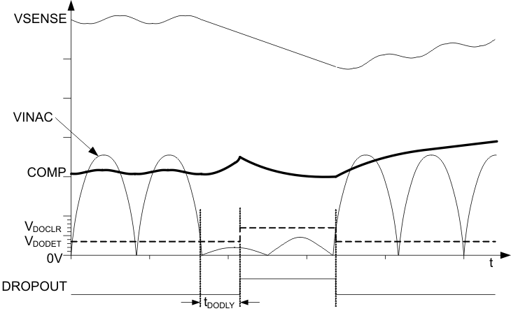 Figure 32. AC-Line Dropout Timing With Illustrative System Behavior
8.3.12 VREF
VREF is an output which supplies a well-regulated reference voltage to circuits within the device as well as serving as a limited source for external circuits. This output must be bypassed to GND with a low-impedance 0.1-μF or larger capacitor placed as close to the VREF and GND pins as possible. Current draw by external circuits should not exceed a few milli-amperes and should not be pulsing.
The VREF output is disabled under the following conditions: when VCC is in UVLO, or when VSENSE is below the Enable threshold. This output can only source current and is unable to accept current into the pin.
8.3.13 VCC
VCC is usually connected to a bias supply of between 13 V and 21 V. To minimize switching ripple voltage on VCC, it should be by-passed with a low-impedance capacitor as close to the VCC and GND pins as possible. The capacitance should be sized to adequately decouple the peak currents due to gate-drive switching at the highest operating frequency. When powered from a poorly-regulated low-impedance supply, an external zener diode is recommended to prevent excessive current into VCC.
The undervoltage-lockout (UVLO) condition is when VCC voltage has not yet reached the turn-on threshold or has fallen below the turn-off threshold, having already been turned on. While in UVLO, the VREF output and most circuits within the device are disabled and VCC current falls significantly below the normal operating level. The same situation applies when VSENSE is below its Enable threshold. This helps minimize power loss during pre-powerup and standby conditions.
8.3.14 Control of Downstream Converter
In the UCC28063A, the PWMCNTL pin can be used to coordinate the PFC stage with a downstream converter. Through the HVSEN pin, the PFC output voltage is monitored. A 12-μA current source (IHV_HYS) is enabled as long as the output voltage remains below a programmed threshold. When the output voltage exceeds that threshold, PWMCNTL pin is pulled to ground internally and can be used to enable a downstream converter. At the same time the current source is disabled, providing hysteresis for a lower threshold at which the downstream converter should be turned off. The enable/disable hysteresis is adjusted through the HVSEN voltage-divider ratio and resistor values. The HVSEN pin is also used for the FailSafe over-voltage protection (OVP). When designing the voltage divider, make sure this FailSafe OVP level is set above normal VSENSE OVP levels.
Because there are two thresholds associated with the HVSEN input detected through a single resistor divider, the PWMCNTL turn-off voltage, VPWM-OFF, is linked to the FailSafe OVP voltage, VFLSF_OV, as shown by Equation 14:

Choosing either one first arbitrarily determines the other, so a trade-off may be necessary. The PWMCNTL turn-on voltage, VPWM-ON, is programmed by choosing the upper divider resistor value in consideration with the HVSEN hysteresis current, as shown in Equation 15 and Equation 16. The lower divider resistor is then calculated as shown in Equation 17.


8.3.15 System Level Protections
8.3.15.1 Failsafe OVP - Output Overvoltage Protection
FailSafe OVP prevents any single failure from allowing the output to boost above safe levels. Redundant paths for output voltage sensing provide additional protection against output over-voltage. Over-voltage protection is implemented through two independent paths: VSENSE and HVSEN. The converter shuts down if either input senses a severe over-voltage condition. The output voltage can still remain below a safe limit if either sense path fails. The device is re-enabled when both sense inputs fall back into their normal ranges. At that time, the gate drive outputs will resume switching under PWM control. A low-level over-voltage on VSENSE does not trigger soft-start, but the COMP pin is discharged by an internal 2-kΩ resistance until the output voltage falls below the 2% hysteresis OV-clear threshold. A higher-level over-voltage on VSENSE additionally shuts off the gate-drive outputs until the OV clears, but still does not trigger a soft-start. However, an overvoltage detected on HVSEN does trigger a full soft-start and the COMP pin is fully discharged to 20 mV before the soft-start can begin.
8.3.15.2 Overcurrent Protection
Under certain conditions (such as inrush, brownout-recovery, and output over-load) the PFC power stage sees large currents. It is critical that the power devices be protected from switching during these conditions.
The conventional current-sensing method uses a shunt resistor in series with each MOSFET source leg to sense the converter currents, resulting in multiple ground points and high power dissipation. Furthermore, since no current information is available when the MOSFETs are off, the source-resistor current-sensing method results in repeated turn-on of the MOSFETs during overcurrent (OC) conditions. Consequently, the converter may temporarily operate in continuous conduction mode (CCM) and may experience failures induced by excessive reverse-recovery currents in the boost diodes or other abnormal stresses.
The UCC28063A uses a single resistor to continuously sense the combined total inductor (input) current. This way, turn-on of the MOSFETs is completely avoided when the inductor currents are excessive. The gate drive to the MOSFETs is inhibited until total inductor current drops to near zero, precluding reverse-recovery-induced failures (these failures are most likely to occur when the ac-line recovers from a brownout condition).
The nominal OC threshold voltage during two-phase operation is -200 mV, which helps minimize losses. This threshold is automatically reduced to -166 mV during single-phase operation, either by detection of a phase failure or because PHB is driven below 0.8 V. Note that the single-phase threshold is not simply 1/2 of the dual-phase threshold, because the ratio of the single-phase peak current to the interleaved peak current is higher than 1/2.
An OC condition immediately turns off both gate-drive outputs, but does not trigger a soft-start and does not modify the error amplifier operation. The over-current condition is cleared when the total inductor current-sense voltage falls below the OC-clear threshold (-15 mV).
Following an over-current condition, both MOSFETs are turned on simultaneously once the input current drops to near zero. Because the two phase currents are temporarily operating in-phase, the current-sense resistance should be chosen so that OC protection is not triggered with twice the maximum current peak value of either phase in order to allow quick return to normal operation after an over-current event. Automatic phase-shift control will re-establish interleaving within a few switching cycles.
8.3.15.3 Open-Loop Protection
If the feedback loop is disconnected from the device, a 100-nA current source internal to the UCC28063A pulls the VSENSE pin voltage towards ground. When VSENSE falls below 1.20 V, the device becomes disabled. When disabled, the bias supply current decreases, both gate-drive outputs and COMP are actively pulled low, and a soft-start condition is initiated. The device is re-enabled when VSENSE rises above 1.25 V. At that time, the gate drive outputs will begin switching under soft-start PWM control.
If the feedback loop is disconnected from ground, the VSENSE voltage will be pulled high. When VSENSE rises above the 2nd-level over-voltage protection threshold, both gate drive outputs are shut off and COMP is actively pulled low. The device is re-enabled when VSENSE falls below the OV-clear threshold. The VSENSE input can tolerate a limited amount of current into the device under abnormally high input voltage conditions. Refer to the Absolute Maximum Ratings table near the beginning of this datasheet for details.
8.3.15.4 VCC Undervoltage Lock-Out (UVLO) Protection
VCC must rise above the turn-on threshold for the PWM to begin functioning. If VCC drops below the UVLO threshold during operation, both gate-drive outputs are actively pulled low, COMP is actively pulled low, and a soft-start condition is triggered. VCC must again rise above the turn-on threshold for the PWM function to restart in soft-start mode.
8.3.15.5 Phase-Fail Protection
The UCC28063A detects failure of either of the phases by monitoring the sequence of ZCD pulses. During normal two-phase operation, if one ZCD input remains idle for longer than approximately 12 ms while the other ZCD input switches normally, the over-current threshold is reduced and PWMCNTL goes to a high-impedance state, indicating that the PFC power stage is not operating correctly. During normal single-phase operation (PHB < 0.8 V), phase failure is not monitored. Also on the UCC28063A, phase failure is not monitored when COMP is below approximately 222 mV.
8.3.15.6 Thermal Shutdown Protection
Overloading of the gate-drive outputs, VREF, or both can dissipate excess power within the device which may raise the internal temperature of the circuits beyond a safe level. Even normal power dissipation can generate excess heat if the thermal impedance is too high or the ambient temperature is too high. When the UCC28063A detects an internal over-temperature condition it will shutdown the outputs and trigger a full soft-start condition. When the internal device junction temperature has cooled below the thermal hysteresis temperature, operation will resume under soft-start control.
8.3.15.7 AC-Line Brownout and Dropout Protections
See specific discussions for each topic in previous sections of this data sheet.
8.3.15.8 Fault Logic Diagram
Figure 33 depicts the fault-handling logic involving VSENSE, COMP, and several internal states.
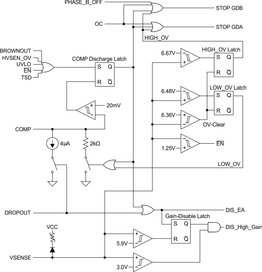 Figure 33. Fault Logic With VSENSE Detections and Error Amplifier Control
8.4 Device Functional Modes
The controller is primarily intended for set up as a dual phase interleaved PFC which utilizes inductor demagnetization information based on inductor sense winding voltages which are routed to ZCDA and ZCDB to trigger the start of a switching cycle.
The functionality may be extended in a couple of ways:
- Phase-B Enable and Disable: Phase-B may be shed by explicit user control or it may be set up as an automatic light load efficiency management feature. When the voltage applied to the PHB pin is below VPHBF threshold, Phase B and the Phase Fail Detector will be disabled. The commanded On-time for Phase-A will be doubled to minimize the output voltage transient which would otherwise occur. When the voltage on the PHB pin is greater than the VPHBR threshold, two phase mode is continuously enabled. Tie PHB to VREF pin for this mode. Alternatively PHB may be tied to the COMP pin for automatic phase shedding at light load.
- PFC Stage Enable and Disable Control: Controller operation is enabled when VSENSE voltage exceeds the 1.25-V enable threshold. The primary disable method should be by pulling VSENSE low by an open drain or open collector logic output. This will disable the outputs and significantly reduce VCC current. Releasing VSENSE will initiate a Soft-Start. Avoid any PCB traces which would couple any noise into this node.