SLUSDW0B May 2020 – May 2020 UCC28065
PRODUCTION DATA.
- 1 Features
- 2 Applications
- 3 Description
- 4 Revision History
- 5 Description (Continued)
- 6 Pin Configuration and Functions
- 7 Specifications
-
8 Detailed Description
- 8.1 Overview
- 8.2 Functional Block Diagram
- 8.3
Feature Description
- 8.3.1 Principles of Operation
- 8.3.2 Natural Interleaving
- 8.3.3 On-Time Control, Maximum Frequency Limiting, Restart Timer and Input Voltage Feed-Forward compensation
- 8.3.4 Zero-Current Detection and Valley Switching
- 8.3.5 Phase Management and Light-Load Operation
- 8.3.6 Burst Mode Operation
- 8.3.7 External Disable
- 8.3.8 Improved Error Amplifier
- 8.3.9 Soft Start
- 8.3.10 Brownout Protection
- 8.3.11 Line Dropout Detection
- 8.3.12 VREF
- 8.3.13 VCC
- 8.3.14
System Level Protections
- 8.3.14.1 Failsafe OVP - Output Over-voltage Protection
- 8.3.14.2 Overcurrent Protection
- 8.3.14.3 Open-Loop Protection
- 8.3.14.4 VCC Undervoltage Lock-Out (UVLO) Protection
- 8.3.14.5 Phase-Fail Protection
- 8.3.14.6 CS - Open, TSET - Open and Short Protection
- 8.3.14.7 Thermal Shutdown Protection
- 8.3.14.8 Fault Logic Diagram
- 8.4 Device Functional Modes
-
9 Application and Implementation
- 9.1 Application Information
- 9.2
Typical Application
- 9.2.1 Design Requirements
- 9.2.2
Detailed Design Procedure
- 9.2.2.1 Inductor Selection
- 9.2.2.2 ZCD Resistor Selection RZA, RZB
- 9.2.2.3 HVSEN
- 9.2.2.4 Output Capacitor Selection
- 9.2.2.5 Selecting RS For Peak Current Limiting
- 9.2.2.6 Power Semiconductor Selection (Q1, Q2, D1, D2)
- 9.2.2.7 Brownout Protection
- 9.2.2.8 Converter Timing
- 9.2.2.9 Programming VOUT
- 9.2.2.10 Voltage Loop Compensation
- 9.2.3 Application Curves
- 10Power Supply Recommendations
- 11Layout
- 12Device and Documentation Support
- 13Mechanical, Packaging, and Orderable Information
8.3.11 Line Dropout Detection
It is often the case that the AC-line voltage momentarily drops to zero or nearly zero, due to transient abnormal events affecting the local AC-power distribution network. Referred to as AC-line dropouts (or sometimes as line-dips) the duration of such events usually extends to only 1 or 2 line cycles. During a dropout, the down-stream power conversion stages depend on sufficient energy storage in the PFC output capacitance, which is sized to provide the ride-through energy for a specified hold-up time. Typically while the PFC output voltage is falling, the voltage-loop error amplifier output rises in an attempt to maintain regulation. As a consequence, excess duty-cycle is commanded when the AC-line voltage returns and high peak current surges may saturate the boost inductors with possible overstress and audible noise.
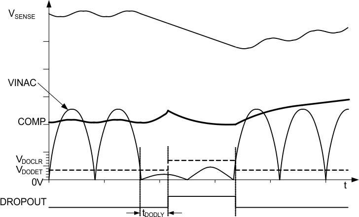
The UCC28065 incorporates a dropout detection feature which suspends the action of the error amplifier for the duration of the dropout. If the VINAC voltage falls below 0.35 V for longer than 5 ms, a dropout condition is detected and the error amplifier output is turned off. In addition, a 4-μA pull down current is applied to COMP to gently discharge the compensation network capacitors. In this way, when the AC-line voltage returns, the COMP voltage (and corresponding duty-cycle setting) remains very near or even slightly below the level it was before the dropout occurred. Current surges due to excess duty-cycle, and their undesired attendant effects, are avoided. The dropout condition is cancelled and the error amplifier resumes normal operation when VINAC rises above 0.71 V.
Based on the VINAC divider-resistor values calculated for Brownout in the previous section, the input RMS voltage thresholds for dropout detection VAC_DO and dropout clearing VDO_CLR can be determined using Equation 17 and Equation 18, below.


Avoid excessive filtering of the VINAC signal, or dropout detection may be delayed or defeated. An RC time-constant of ≤ 100 s. should provide good performance. Figure 29 shows an example of the timing for the dropout function.
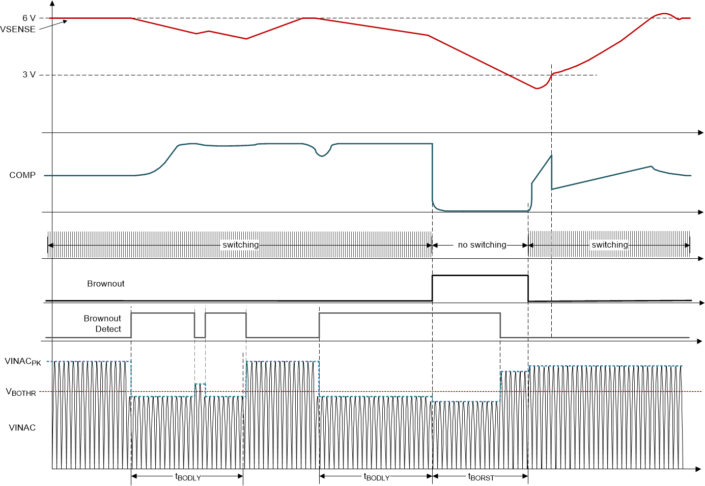
 Figure 28. AC-Line Brownout Timing and System Behavior
  Figure 29. AC-Line Dropout Timing With Illustrative System Behavior