SLUS829G August 2008 – February 2020 UCC2897A
PRODUCTION DATA.
- 1 Features
- 2 Applications
- 3 Description
- 4 Revision History
- 5 Device Options
- 6 Pin Configuration and Functions
- 7 Specifications
-
8 Detailed Description
- 8.1 Overview
- 8.2 Functional Block Diagram
- 8.3 Feature Description
- 8.4 Device Functional Modes
- 9 Application and Implementation
- 10Power Supply Recommendations
- 11Layout
- 12Device and Documentation Support
- 13Mechanical, Packaging, and Orderable Information
パッケージ・オプション
メカニカル・データ(パッケージ|ピン)
サーマルパッド・メカニカル・データ
- RGP|20
発注情報
8.3.8 Bootstrap Biasing
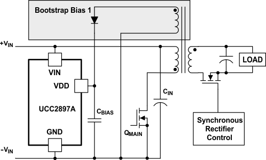
Many converters use a bootstrap circuit to generate bias power during steady-state operation. The popularity of this solution is justified by the simplicity and high-efficiency of the circuit. Usually, bias power is derived from the main transformer by adding an additional dedicated winding to the structure. Using a flyback converter as shown in Figure 25, a bootstrap winding provides a quasi-regulated bias voltage for the primary-side control circuits. The voltage on the VDD pin is equal to the output voltage times the turns-ratio between the output and the bootstrap-winding in the transformer. Because the output is regulated, the bias rail is regulated as well.
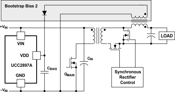
While the same arrangement is used in a forward-type converter, the bootstrap winding off the main-power transformer is unable to provide a quasi-regulated voltage. In the forward converter, the voltage across the bootstrap-winding equals the input voltage times the turns-ratio. Accordingly the bias voltage would vary with the input voltage and exceeds the maximum-operating voltage of the control circuits at high line. A linear regulator limits and regulates the bias voltage if the power dissipation is acceptable. Another possible solution for the forward converter is to generate the bias voltage from the output inductor as shown in Figure 26.
 Figure 25. Bootstrap Bias 1, Flyback Example
 This solution uses the regulated output voltage across the output inductor during the freewheeling period to generate a quasi-regulated bias for the control circuits.
 Figure 26. Bootstrap Bias 2, Forward Example
 This solution uses the regulated output voltage across the output inductor during the freewheeling period to generate a quasi-regulated bias for the control circuits.
Both of the illustrated solutions provide reliable bias-power during normal operation. Note that in both cases, the bias voltages are proportional to the output voltage. This nature of the bootstrap bias-supply causes the converter to operate in a hiccup mode under significant overload or under short-circuit conditions as the bootstrap winding is not able to hold the bias rail above the undervoltage lockout-threshold of the controller.
Another biasing solution, based on the active circuit, is shown on the previous page with components Q10, C18, R19, D10 and D12. Such a circuit is used in the applications where the allowed biasing-capacitor size is limited to optimize the board space utilization.