JAJSCI5B august 2016 – march 2022 UCD9090A
PRODUCTION DATA
- 1
- 1 特長
- 2 アプリケーション
- 3 概要
- 4 Revision History
- 5 Pin Configuration and Functions
- 6 Specifications
-
7 Detailed Description
- 7.1 Overview
- 7.2 Functional Block Diagram
- 7.3 Feature Description
- 7.4
Device Functional Modes
- 7.4.1 Power Supply Sequencing
- 7.4.2 Pin-Selected Rail States
- 7.4.3 Monitoring
- 7.4.4 Fault Responses and Alert Processing
- 7.4.5 Shut Down All Rails and Sequence On (Resequence)
- 7.4.6 GPIOs
- 7.4.7 GPO Control
- 7.4.8 GPO Dependencies
- 7.4.9 GPI Special Functions
- 7.4.10 Power Supply Enables
- 7.4.11 Cascading Multiple Devices
- 7.4.12 PWM Outputs
- 7.4.13 Programmable Multiphase PWMs
- 7.4.14 Margining
- 7.4.15 Run Time Clock
- 7.4.16 System Reset Signal
- 7.4.17 Watch Dog Timer
- 7.4.18 Data and Error Logging to Flash Memory
- 7.4.19 Brownout Function
- 7.4.20 PMBus Address Selection
- 7.4.21 Device Reset
- 7.4.22 JTAG Interface
- 7.4.23 Internal Fault Management and Memory Error Correction (ECC)
- 7.5 Programming
- 8 Application and Implementation
- 9 Power Supply Recommendations
- 10Layout
- 11Device and Documentation Support
- 12Mechanical, Packaging, and Orderable Information
パッケージ・オプション
デバイスごとのパッケージ図は、PDF版データシートをご参照ください。
メカニカル・データ(パッケージ|ピン)
- RGZ|48
サーマルパッド・メカニカル・データ
- RGZ|48
発注情報
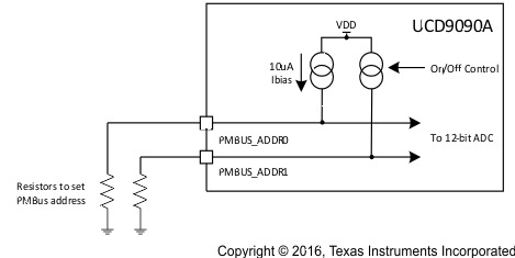
7.4.20 PMBus Address Selection
Two pins are allocated to decode the PMBus address. At power up, the device applies a bias current to each address-detect pin, and the voltage on that pin is captured by the internal 12-bit ADC. The PMBus address is calculated as follows.
where
- bin(VAD0x) is the address bin for one of eight addresses as shown in Table 7-11
The address bins are defined by the MIN and MAX VOLTAGE RANGE (V). Each bin is a constant ratio of 1.25 from the previous bin. This method maintains the width of each bin relative to the tolerance of standard 1% resistors.
| ADDRESS BIN | RPMBus PMBus RESISTANCE (kΩ) |
|---|---|
| open | — |
| 11 | 200 |
| 10 | 154 |
| 9 | 118 |
| 8 | 90.9 |
| 7 | 69.8 |
| 6 | 53.6 |
| 5 | 41.2 |
| 4 | 31.6 |
| short | — |
A low impedance (short) on either address pin that produces a voltage below the minimum voltage causes the PMBus address to default to address 126 (0x7E). A high impedance (open) on either address pin that produces a voltage above the maximum voltage also causes the PMBus address to default to address 126 (0x7E).
Address 0 is not used because it is the PMBus general-call address. Addresses 11 and 127 can not be used by this device or any other device that shares the PMBus with it, because those are reserved for manufacturing programming and test. It is recommended that address 126 not be used for any devices on the PMBus, because this is the address that the UCD9090A defaults to if the address lines are shorted to ground or left open. Table 7-12 summarizes which PMBus addresses can be used. Other SMBus/PMBus addresses have been assigned for specific devices. For a system with other types of devices connected to the same PMBus, see the SMBus device address assignments table in Appendix C of the latest version of the System Management Bus (SMBus) specification. The SMBus specification can be downloaded at http://smbus.org/specs/smbus20.pdf.
| ADDRESS | STATUS | REASON |
|---|---|---|
| 0 | Prohibited | SMBus generaladdress call |
| 11 | Avoid | Causes conflicts with other devices during program flash updates. |
| 12 | Prohibited | PMBus alert response protocol |
| 126 | For JTAG Use | Default value; may cause conflicts with other devices. |
| 127 | Prohibited | Used by TI manufacturing for device tests. |
 Figure 7-27 PMBus Address-Detection Method
Address 126 (0x7E) is not recommended to be selected as a permanent PMBus address for any given application design. Leaving the address in default state as 126 (0x7E) will enable the JTAG and not allow using the JTAG compatible pins (27-30) as GPIOs. The UCD9090A runs at 10% slower frequency while the JTAG is enabled to ensure best JTAG operation.