JAJSCI5B august 2016 – march 2022 UCD9090A
PRODUCTION DATA
- 1
- 1 特長
- 2 アプリケーション
- 3 概要
- 4 Revision History
- 5 Pin Configuration and Functions
- 6 Specifications
-
7 Detailed Description
- 7.1 Overview
- 7.2 Functional Block Diagram
- 7.3 Feature Description
- 7.4
Device Functional Modes
- 7.4.1 Power Supply Sequencing
- 7.4.2 Pin-Selected Rail States
- 7.4.3 Monitoring
- 7.4.4 Fault Responses and Alert Processing
- 7.4.5 Shut Down All Rails and Sequence On (Resequence)
- 7.4.6 GPIOs
- 7.4.7 GPO Control
- 7.4.8 GPO Dependencies
- 7.4.9 GPI Special Functions
- 7.4.10 Power Supply Enables
- 7.4.11 Cascading Multiple Devices
- 7.4.12 PWM Outputs
- 7.4.13 Programmable Multiphase PWMs
- 7.4.14 Margining
- 7.4.15 Run Time Clock
- 7.4.16 System Reset Signal
- 7.4.17 Watch Dog Timer
- 7.4.18 Data and Error Logging to Flash Memory
- 7.4.19 Brownout Function
- 7.4.20 PMBus Address Selection
- 7.4.21 Device Reset
- 7.4.22 JTAG Interface
- 7.4.23 Internal Fault Management and Memory Error Correction (ECC)
- 7.5 Programming
- 8 Application and Implementation
- 9 Power Supply Recommendations
- 10Layout
- 11Device and Documentation Support
- 12Mechanical, Packaging, and Orderable Information
パッケージ・オプション
デバイスごとのパッケージ図は、PDF版データシートをご参照ください。
メカニカル・データ(パッケージ|ピン)
- RGZ|48
サーマルパッド・メカニカル・データ
- RGZ|48
発注情報
7.4.19 Brownout Function
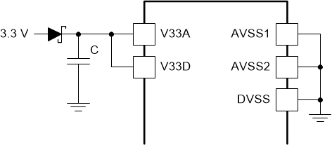
The UCD9090A can be enabled to turn off all nonvolatile logging until a brownout event is detected. A brownout event occurs if VCC drops below 2.9 V. In order to enable this feature, the user must provide enough local capacitance to deliver up to 80 mA (consider additional load based on GPOs sourcing external circuits such as LEDs) on for 5 ms while maintaining a minimum of 2.6 V at the device. If using the brownout circuit (Figure 7-26), then a schottky diode should be placed so that it blocks the other circuits that are also powered from the 3.3 V supply.
With this feature enabled, the UCD9090A saves faults, peaks, and other log data to SRAM during normal operation of the device. Once a brownout event is detected, all data is copied from SRAM to Flash if the log is not disabled. Use of this feature allows the UCD9090A to keep track of a single run-time clock that spans device resets or system power down (rather than resetting the run time clock after device reset). It can also improve the UCD9090A internal response time to events, because Flash writes are disabled during normal system operation. This is an optional feature and can be enabled using the MISC_CONFIG command. For more details, see the UCD90xxx Sequencer and System Health Controller PMBus Command Reference.
 Figure 7-26 Brownout Circuit