SLVSC86A January 2014 – March 2014 UCD9244-EP
PRODUCTION DATA.
- 1 Features
- 2 Applications
- 3 Description
- 4 Revision History
- 5 Description (Continued)
- 6 Terminal Configuration and Functions
-
7 Specifications
- 7.1 Absolute Maximum Ratings
- 7.2 Handling Ratings
- 7.3 Recommended Operating Conditions
- 7.4 Thermal Information
- 7.5 Electrical Characteristics
- 7.6 Electrical Characteristics (Continued)
- 7.7 ADC Monitoring Intervals And Response Times
- 7.8 Hardware Fault Detection Latency
- 7.9 PMBus/SMBus/I2C
- 7.10 I2C/SMBus/PMBus Timing Requirements
- 7.11 Typical Characteristics
-
8 Detailed Description
- 8.1 Overview
- 8.2 Functional Block Diagram
- 8.3
Feature Description
- 8.3.1 PMBus Interface
- 8.3.2 Resistor Programmed PMBus Address Decode
- 8.3.3 VID Interface
- 8.3.4 Jtag Interface
- 8.3.5 Bias Supply Generator (Shunt Regulator Controller)
- 8.3.6 Power-On Reset
- 8.3.7 External Reset
- 8.3.8 ON_OFF_CONFIG
- 8.3.9 Output Voltage Adjustment
- 8.3.10 Calibration
- 8.3.11 Analog Front End (AFE)
- 8.3.12 Voltage Sense Filtering
- 8.3.13 DPWM Engine
- 8.3.14 Rail/Power Stage Configuration
- 8.3.15 DPWM Phase Synchronization
- 8.3.16 Output Current Measurement
- 8.3.17 Current Sense Input Filtering
- 8.3.18 Over-Current Detection
- 8.3.19 Input Voltage Monitoring
- 8.3.20 Input UV Lockout
- 8.3.21 Temperature Monitoring
- 8.3.22 Auxiliary ADC Input Monitoring
- 8.3.23 Soft Start, Soft Stop Ramp Sequence
- 8.3.24 Non-Volatile Memory Error Correction Coding
- 8.3.25 Data Logging
- 8.4 Device Functional Modes
- 9 Applications and Implementation
- 10Power Supply Recommendations
- 11Layout
- 12Device and Documentation Support
- 13Mechanical, Packaging, and Orderable Information
パッケージ・オプション
メカニカル・データ(パッケージ|ピン)
- RGC|64
サーマルパッド・メカニカル・データ
- RGC|64
発注情報
8.3.2 Resistor Programmed PMBus Address Decode
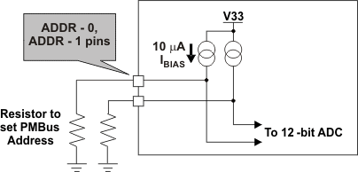
The PMBus Address is selected using resistors attached to the ADDR0 and ADDR1 terminals. At power-up, the device applies a bias current to each address detect terminal. The measured voltage on each terminal determines the PMBus address as defined in Table 1. For example, a 133kΩ resistor on ADDR1 and a 75kΩ on ADDR0 will select PMBus address = 100. Resistors are chosen from the standard EIA-E96 series, and should have accuracy of 1% or better.
 Figure 4. PMBus Address Detection Method
A short or open on either address terminal causes the PMBus address to default to address 126. To avoid potential conflicts between multiple devices, it is best to avoid using address 126.
Some addresses should be avoided; see Table 1 for details.
Table 1. PMBus Address Bins(1)
| ADDR0 | |||||||||||||||
| (short) < 36.5k |
42.2k | 48.7k | 56.2k | 64.9k | 75k | 86.6k | 100k | 115k | 133k | 154k | 178k | 205k | (open) > 237k |
||
 |
< 36.5k (short) |
126 | 126 | 126 | 126 | 126 | 126 | 126 | 126 | 126 | 126 | 126 | 126 | 126 | 126 |
| 42.2k | 126 | 126(2) | 1 | 2 | 3 | 4 | 5 | 6 | 7 | 8 | 9 | 10 | 11(3) | 126 | |
| 48.7k | 126 | 126(2) | 13 | 14 | 15 | 16 | 17 | 18 | 19 | 20 | 21 | 22 | 33 | 126 | |
| 56.2k | 126 | 24 | 25 | 26 | 27 | 28 | 29 | 30 | 31 | 32 | 33 | 34 | 35 | 126 | |
| 64.9k | 126 | 36 | 37 | 38 | 39 | 40 | 41 | 42 | 43 | 44 | 45 | 46 | 47 | 126 | |
| 75k | 126 | 48 | 49 | 50 | 51 | 52 | 53 | 54 | 55 | 56 | 57 | 58 | 59 | 126 | |
| 86.6k | 126 | 60 | 61 | 62 | 63 | 64 | 65 | 66 | 67 | 68 | 69 | 70 | 71 | 126 | |
| 100k | 126 | 72 | 73 | 74 | 75 | 76 | 77 | 78 | 79 | 80 | 81 | 82 | 83 | 126 | |
| 115k | 126 | 84 | 85 | 86 | 87 | 88 | 89 | 90 | 91 | 92 | 93 | 94 | 95 | 126 | |
| 133k | 126 | 96 | 97 | 98 | 99 | 100 | 101 | 102 | 103 | 104 | 105 | 106 | 107 | 126 | |
| 154k | 126 | 108 | 109 | 110 | 111 | 112 | 113 | 114 | 115 | 116 | 117 | 118 | 119 | 126 | |
| 178k | 126 | 120 | 121 | 122 | 123 | 124 | 125 | 126 | 126(2) | 126 | 126 | 126 | 126 | 126 | |
| 205k | 126 | 126 | 126 | 126 | 126 | 126 | 126 | 126 | 126 | 126 | 126 | 126 | 126 | 126 | |
| > 237k (open) |
126 | 126 | 126 | 126 | 126 | 126 | 126 | 126 | 126 | 126 | 126 | 126 | 126 | 126 | |