SLVSC86A January 2014 – March 2014 UCD9244-EP
PRODUCTION DATA.
- 1 Features
- 2 Applications
- 3 Description
- 4 Revision History
- 5 Description (Continued)
- 6 Terminal Configuration and Functions
-
7 Specifications
- 7.1 Absolute Maximum Ratings
- 7.2 Handling Ratings
- 7.3 Recommended Operating Conditions
- 7.4 Thermal Information
- 7.5 Electrical Characteristics
- 7.6 Electrical Characteristics (Continued)
- 7.7 ADC Monitoring Intervals And Response Times
- 7.8 Hardware Fault Detection Latency
- 7.9 PMBus/SMBus/I2C
- 7.10 I2C/SMBus/PMBus Timing Requirements
- 7.11 Typical Characteristics
-
8 Detailed Description
- 8.1 Overview
- 8.2 Functional Block Diagram
- 8.3
Feature Description
- 8.3.1 PMBus Interface
- 8.3.2 Resistor Programmed PMBus Address Decode
- 8.3.3 VID Interface
- 8.3.4 Jtag Interface
- 8.3.5 Bias Supply Generator (Shunt Regulator Controller)
- 8.3.6 Power-On Reset
- 8.3.7 External Reset
- 8.3.8 ON_OFF_CONFIG
- 8.3.9 Output Voltage Adjustment
- 8.3.10 Calibration
- 8.3.11 Analog Front End (AFE)
- 8.3.12 Voltage Sense Filtering
- 8.3.13 DPWM Engine
- 8.3.14 Rail/Power Stage Configuration
- 8.3.15 DPWM Phase Synchronization
- 8.3.16 Output Current Measurement
- 8.3.17 Current Sense Input Filtering
- 8.3.18 Over-Current Detection
- 8.3.19 Input Voltage Monitoring
- 8.3.20 Input UV Lockout
- 8.3.21 Temperature Monitoring
- 8.3.22 Auxiliary ADC Input Monitoring
- 8.3.23 Soft Start, Soft Stop Ramp Sequence
- 8.3.24 Non-Volatile Memory Error Correction Coding
- 8.3.25 Data Logging
- 8.4 Device Functional Modes
- 9 Applications and Implementation
- 10Power Supply Recommendations
- 11Layout
- 12Device and Documentation Support
- 13Mechanical, Packaging, and Orderable Information
パッケージ・オプション
メカニカル・データ(パッケージ|ピン)
- RGC|64
サーマルパッド・メカニカル・データ
- RGC|64
発注情報
8.3.12 Voltage Sense Filtering
Conditioning should be provided on the EAP and EAN signals. Figure 9 shows a divider network between the output voltage and the voltage sense input to the controller. The resistor divider is used to bring the output voltage within the dynamic range of the controller. When no attenuation is needed, R2 can be left open and the signal conditioned by the low-pass filter formed by R1 and C2.
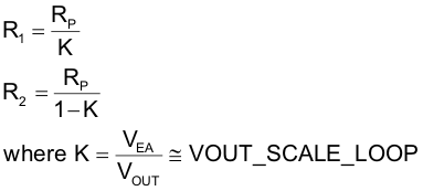
As with any power supply system, maximize the accuracy of the output voltage by sensing the voltage directly across an output capacitor as close to the load as possible. Route the positive and negative differential sense signals as a balanced pair of traces or as a twisted pair cable back to the controller. Put the divider network close to the controller. This ensures that there is low impedance driving the differential voltage sense signal from the voltage rail output back to the controller. The resistance of the divider network is a trade-off between power loss and minimizing interference susceptibility. A parallel resistance (Rp) of 1kΩ to 4kΩ is a good compromise. Once RP is chosen, R1 and R2 can be determined from the following formulas.

It is recommended that a capacitor be placed across the lower resistor of the divider network. This acts as an additional pole in the compensation and as an anti-alias filter for the EADC. To be effective as an anti-alias filter, the corner frequency should be 35% to 40% of the switching frequency. Then the capacitor is calculated as:

To obtain the best possible accuracy, the input resistance and offset current on the device should be considered when calculating the gain of a voltage divider between the output voltage and the EA sense inputs of the UCD9244. The input resistance and input offset current are specified in the parametric tables in this datasheet. VEA = VEAP – VEAN in the equation below.

The effect of the offset current can be reduced by making the resistance of the divider network low.