SLRS060C May 2012 – November 2016 ULN2003V12
PRODUCTION DATA.
- 1 Features
- 2 Applications
- 3 Description
- 4 Revision History
- 5 Pin Configuration and Functions
- 6 Specifications
- 7 Detailed Description
- 8 Applications and Implementation
- 9 Power Supply Recommendations
- 10Layout
- 11Device and Documentation Support
- 12Mechanical, Packaging, and Orderable Information
パッケージ・オプション
メカニカル・データ(パッケージ|ピン)
サーマルパッド・メカニカル・データ
発注情報
10 Layout
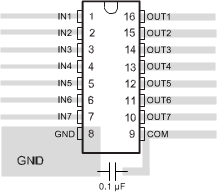
10.1 Layout Guidelines
Thin traces can be used on the input due to the low current logic that is typically used to drive ULN2003V12. Take care to separate the input channels as much as possible, as to eliminate cross-talk. TI recommends thick traces for the output to drive high currents that may be required. Wire thickness can be determined by the trace material's current density and desired drive current. Because all of the channels currents return to a common ground, it is best to size that trace width to be very wide. Some applications require up to 1 A.
10.2 Layout Example

10.3 Thermal Considerations
10.3.1 On-chip Power Dissipation
Use Equation 3 to calculate ULN2003V12 on-chip power dissipation PD.

where
- N is the number of channels active together
- VOLi is the OUTi pin voltage for the load current ILi
10.3.2 Thermal Reliability
TI recommends limiting the ULN2003V12 IC’s die junction temperature to less than 125°C. The IC junction temperature is directly proportional to the on-chip power dissipation. Use Equation 4 to calculate the maximum allowable on-chip power dissipation for a target IC junction temperature.

where
- TJ(MAX) is the target maximum junction temperature
- TA is the operating ambient temperature
- θJA is the package junction to ambient thermal resistance