JAJSHP9E November 2007 – July 2019 VCA824
PRODUCTION DATA.
- 1 特長
- 2 アプリケーション
- 3 概要
- 4 改訂履歴
- 5 Device Comparison Table
- 6 Pin Configuration and Functions
-
7 Specifications
- 7.1 Absolute Maximum Ratings
- 7.2 ESD Ratings
- 7.3 Recommended Operating Conditions
- 7.4 Thermal Information
- 7.5 Electrical Characteristics: VS = ±5 V
- 7.6 Typical Characteristics: VS = ±5 V, AVMAX = 2 V/V
- 7.7 Typical Characteristics: VS = ±5 V, AVMAX = 10 V/V
- 7.8 Typical Characteristics: VS = ±5 V, AVMAX = 40 V/V
- 8 Detailed Description
- 9 Application and Implementation
- 10Power Supply Recommendations
- 11Layout
- 12デバイスおよびドキュメントのサポート
- 13メカニカル、パッケージ、および注文情報
パッケージ・オプション
メカニカル・データ(パッケージ|ピン)
サーマルパッド・メカニカル・データ
発注情報
7.6 Typical Characteristics: VS = ±5 V, AVMAX = 2 V/V
At TA = 25°C, RL = 100 Ω, RF = 453 Ω, RG = 453 Ω, VG = 1 V, VIN = single-ended input on +VIN with –VIN at ground, and 14-Pin SOIC package, unless otherwise noted.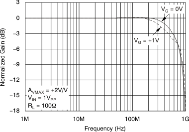 Figure 1. Small-Signal Frequency Response
  Figure 3. Small-Signal Pulse Response
  Figure 5. Composite Video dG/dP
  Figure 7. Harmoneic Distortion vs Frequency
 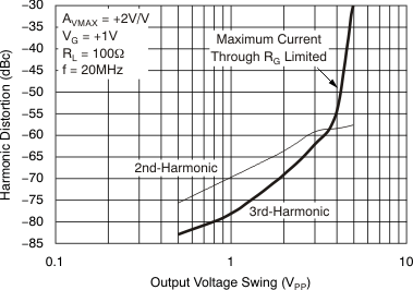 Figure 9. Harmonic Distortion vs Output Voltage
  Figure 11. Two-Tone, 3rd-Order Intermodulation Intercept
 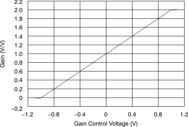 Figure 13. Gain vs Gain Control Voltage
  Figure 15. Gain Control Pulse Response
 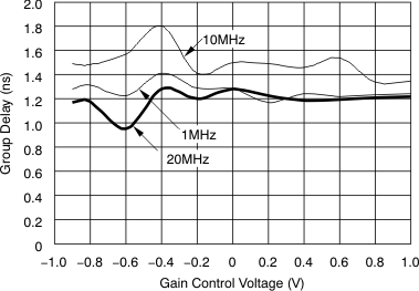 Figure 17. Group Delay vs Gain Control Voltage
  Figure 19. Recommended RSvs Capacitive Load
  Figure 21. Output Voltage Density
 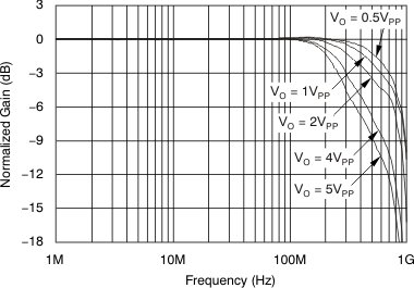 Figure 2. Large-Signal Frequency Response
  Figure 4. Large-Signal Pulse Response
 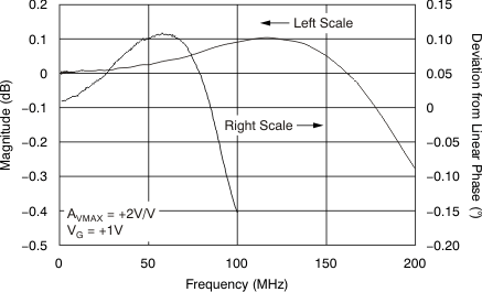 Figure 6. Gain Flatness, Deviation From Linear Phase
 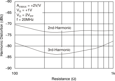 Figure 8. Harmonic Distortion vs Load Resistance
 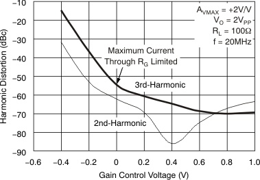 Figure 10. Harmonic Distortion vs Gain Control Voltage
  Figure 12. Two-Tone, 3rd-Order Intermodulation Intercept vs Gain Control Voltage
  Figure 14. Gain Control Frequency Response
  Figure 16. Fully-Attenuated Response
  Figure 18. Group Delay vs Frequency
  Figure 20. Frequency Response vs Capacitive Load
  Figure 22. Input Current Noise Density