JAJSHP9E November 2007 – July 2019 VCA824
PRODUCTION DATA.
- 1 特長
- 2 アプリケーション
- 3 概要
- 4 改訂履歴
- 5 Device Comparison Table
- 6 Pin Configuration and Functions
-
7 Specifications
- 7.1 Absolute Maximum Ratings
- 7.2 ESD Ratings
- 7.3 Recommended Operating Conditions
- 7.4 Thermal Information
- 7.5 Electrical Characteristics: VS = ±5 V
- 7.6 Typical Characteristics: VS = ±5 V, AVMAX = 2 V/V
- 7.7 Typical Characteristics: VS = ±5 V, AVMAX = 10 V/V
- 7.8 Typical Characteristics: VS = ±5 V, AVMAX = 40 V/V
- 8 Detailed Description
- 9 Application and Implementation
- 10Power Supply Recommendations
- 11Layout
- 12デバイスおよびドキュメントのサポート
- 13メカニカル、パッケージ、および注文情報
パッケージ・オプション
メカニカル・データ(パッケージ|ピン)
サーマルパッド・メカニカル・データ
発注情報
7.8 Typical Characteristics: VS = ±5 V, AVMAX = 40 V/V
At TA = 25°C, RL = 100 Ω, RF = 402 Ω, RG = 18 Ω, VG = 1 V, VIN = single-ended input on +VIN with –VIN at ground, and SO-14 package, unless otherwise noted.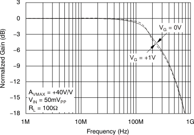 Figure 44. Small-Signal Frequency Response
 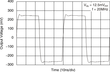 Figure 46. Small-Signal Pulse Response
 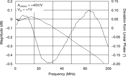 Figure 48. Gain Flatness, Deviation from Linear Phase
 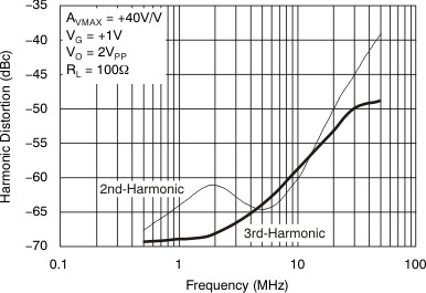 Figure 50. Harmonic Distortion vs Frequency
 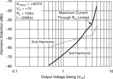 Figure 52. Harmonic Distortion vs Output Voltage
 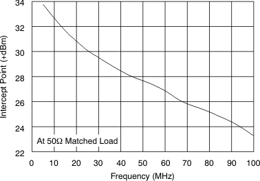 Figure 54. Two-Tone, 3rd-Order Intermodulation Intercept
 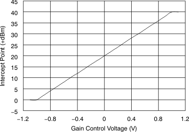 Figure 56. Gain vs Gain Control Voltage
 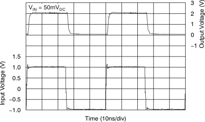 Figure 58. Gain Control Pulse Response
 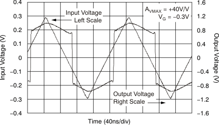 Figure 60. IRG Limited Overdrive Recovery
 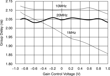 Figure 62. Group Delay vs Gain Control Voltage
 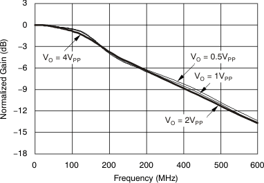 Figure 45. Large-Signal Frequency Response
 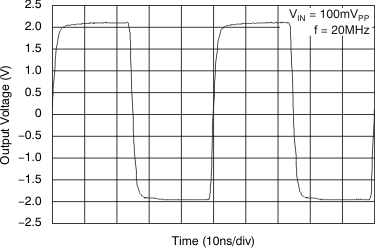 Figure 47. Large-Signal Pulse Response
 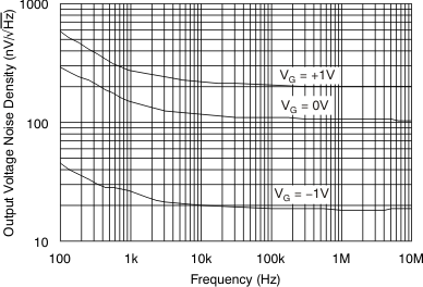 Figure 49. Output Voltage Noise Density
 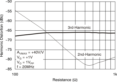 Figure 51. Harmonic Distortion vs Load Resistance
 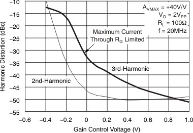 Figure 53. Harmonic Distortion vs Gain Control Voltage
 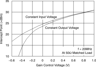 Figure 55. Two-Tone, 3rd-Order Intermodulation Intercept vs Gain Control Voltage
 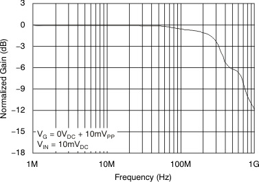 Figure 57. Gain Control Frequency Response
 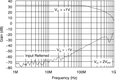 Figure 59. Fully Attenuated Response
 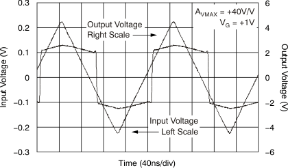 Figure 61. Output Limited Overdrive Recovery
 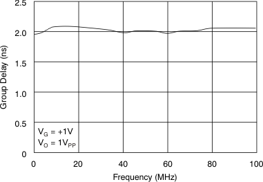 Figure 63. Group Delay vs Frequency