JAJSHP9E November 2007 – July 2019 VCA824
PRODUCTION DATA.
- 1 特長
- 2 アプリケーション
- 3 概要
- 4 改訂履歴
- 5 Device Comparison Table
- 6 Pin Configuration and Functions
-
7 Specifications
- 7.1 Absolute Maximum Ratings
- 7.2 ESD Ratings
- 7.3 Recommended Operating Conditions
- 7.4 Thermal Information
- 7.5 Electrical Characteristics: VS = ±5 V
- 7.6 Typical Characteristics: VS = ±5 V, AVMAX = 2 V/V
- 7.7 Typical Characteristics: VS = ±5 V, AVMAX = 10 V/V
- 7.8 Typical Characteristics: VS = ±5 V, AVMAX = 40 V/V
- 8 Detailed Description
- 9 Application and Implementation
- 10Power Supply Recommendations
- 11Layout
- 12デバイスおよびドキュメントのサポート
- 13メカニカル、パッケージ、および注文情報
パッケージ・オプション
メカニカル・データ(パッケージ|ピン)
サーマルパッド・メカニカル・データ
発注情報
9.1.1 Difference Amplifier
Because both inputs of the VCA824 are high-impedance, a difference amplifier can be implemented without any major problem. Figure 65 shows this implementation. This circuit provides excellent common-mode rejection ratio (CMRR) as long as the input is within the CMRR range of –2.1 V to 1.6 V. Note that this circuit does not make use of the gain control pin, VG. Also, it is recommended to choose RS such that the pole formed by RS and the parasitic input capacitance does not limit the bandwidth of the circuit. Figure 66 shows the common-mode rejection ratio for this circuit implemented in a gain of 10 V/V for VG = 1 V. Note that because the gain control voltage is fixed and is normally set to 1V, the feedback element can be reduced in order to increase the bandwidth. When reducing the feedback element, make sure that the VCA824 is not limited by common-mode input voltage, the current flowing through RG, or any other limitation described in this data sheet.
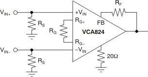 Figure 65. Difference Amplifier
 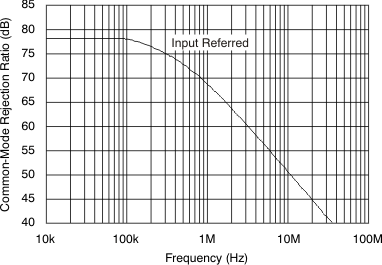 Figure 66. Common-Mode Rejection Ratio
 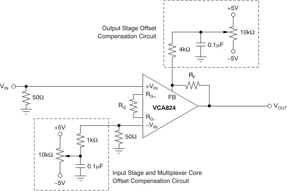 Figure 67. Adjusting the Input and Output Voltage Sources
 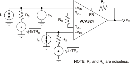 Figure 68. Simple Noise Model
 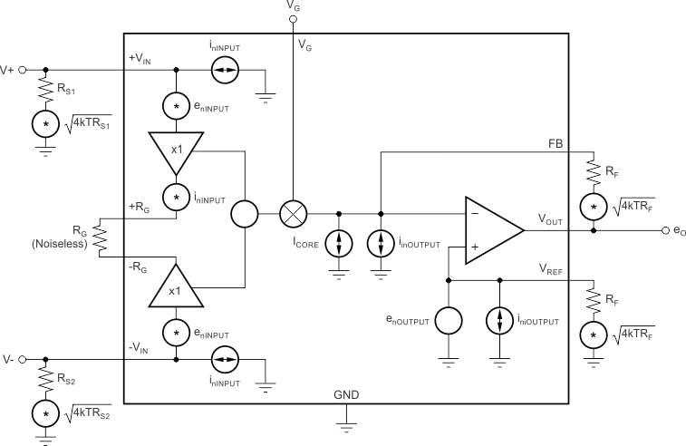 Figure 69. Full Noise Model