JAJSHP9E November 2007 – July 2019 VCA824
PRODUCTION DATA.
- 1 特長
- 2 アプリケーション
- 3 概要
- 4 改訂履歴
- 5 Device Comparison Table
- 6 Pin Configuration and Functions
-
7 Specifications
- 7.1 Absolute Maximum Ratings
- 7.2 ESD Ratings
- 7.3 Recommended Operating Conditions
- 7.4 Thermal Information
- 7.5 Electrical Characteristics: VS = ±5 V
- 7.6 Typical Characteristics: VS = ±5 V, AVMAX = 2 V/V
- 7.7 Typical Characteristics: VS = ±5 V, AVMAX = 10 V/V
- 7.8 Typical Characteristics: VS = ±5 V, AVMAX = 40 V/V
- 8 Detailed Description
- 9 Application and Implementation
- 10Power Supply Recommendations
- 11Layout
- 12デバイスおよびドキュメントのサポート
- 13メカニカル、パッケージ、および注文情報
パッケージ・オプション
メカニカル・データ(パッケージ|ピン)
サーマルパッド・メカニカル・データ
発注情報
9.1.4 Voltage-Controlled Lowpass Filter [application sub]
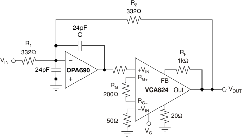
In the circuit of Figure 74, the VCA824 serves as the variable-gain element of a voltage-controlled low-pass filter. This section discusses how this implementation expands the circuit voltage swing capability over that normally achieved with the equivalent multiplier implementation. The circuit control voltage, VG, is calculated as according to the simplified relationship described in Equation 6.

 Figure 74. Voltage-Control Low-Pass Filter
 The response control results from amplification of the feedback voltage applied to R2. First, consider the case where the VCA824 produces G = 1V/V. Then this circuit performs as if the amplifier were replaced by a short circuit. Visually replacing the amplifier by a short leaves a simple voltage-feedback amplifier with a feedback resistor bypassed by a capacitor. Replacing this gain with a variable gain, G, the pole can be written as shown in Equation 7.

Because the VCA824 is most linear in the midrange, the median of the adjustable pole should be set at VG = 0V (see Figure 13, Figure 33, Figure 54, and Equation 8). Selecting R1 = R2 = 332Ω, and targeting a median frequency of 10MHz, the capacitance (C) is 24pF. Because the OPA690 was selected for the circuit of Figure 74, and in order to limit peaking in the OPA690 frequency response, a capacitor equal to C was added on the inverting mode to ground. This architecture has the effect of setting the high-frequency noise gain of the OPA690 to 2V/V, ensuring stability and providing flat frequency response.

Once the median frequency is set, the maximum and minimum frequencies can be determined by using VG = –0.8 V and VG = 0.8 V in the gain equation of Equation 9. Note that this is a first-order analysis and does not take into consideration the open-loop gain limitation of the OPA690.

With the components shown, the circuit provides a linear variation of the low-pass cutoff from 2MHz to 20MHz, using –1V ≤ VG ≤ 1V.