JAJS366D October   2006  – October 2024 XTR111

PRODUCTION DATA  

  1.   1
  2. 特長
  3. アプリケーション
  4. 概要
  5. Pin Configurations and Functions
  6. Specifications
    1. 5.1 Absolute Maximum Ratings
    2. 5.2 ESD Ratings
    3. 5.3 Recommended Operating Conditions
    4. 5.4 Thermal Information
    5. 5.5 Electrical Characteristics
    6. 5.6 Typical Characteristics
  7. Detailed Description
    1. 6.1 Overview
    2. 6.2 Functional Block Diagram
    3. 6.3 Feature Description
      1. 6.3.1 Explanation of Pin Functions
      2. 6.3.2 Dynamic Performance
      3. 6.3.3 External Current Limit
      4. 6.3.4 External MOSFET
      5. 6.3.5 Output Error Flag and Disable Input
      6. 6.3.6 Voltage Regulator
      7. 6.3.7 Level Shift of 0V Input and Transconductance Trim
    4. 6.4 Device Functional Modes
  8. Application and Implementation
    1. 7.1 Application Information
      1. 7.1.1 Input Voltage
      2. 7.1.2 Error Flag Delay
      3. 7.1.3 Voltage Output Configuration
      4. 7.1.4 4mA-to-20mA Output
    2. 7.2 Typical Applications
      1. 7.2.1 0mA–20mA Voltage-to-Current Converter
        1. 7.2.1.1 Design Requirements
        2. 7.2.1.2 Detailed Design Procedure
        3. 7.2.1.3 Application Curve
      2. 7.2.2 Additional Applications
    3. 7.3 Power Supply Recommendations
    4. 7.4 Layout
      1. 7.4.1 Layout Guidelines
        1. 7.4.1.1 Package and Heat Dissipation
        2. 7.4.1.2 Thermal Pad Guidelines
      2. 7.4.2 Layout Example
  9. Device and Documentation Support
    1. 8.1 Device Support
      1. 8.1.1 サード・パーティ製品に関する免責事項
    2. 8.2 Documentation Support
      1. 8.2.1 Related Documentation
    3. 8.3 ドキュメントの更新通知を受け取る方法
    4. 8.4 サポート・リソース
    5. 8.5 Trademarks
    6. 8.6 静電気放電に関する注意事項
    7. 8.7 用語集
  10. Revision History
  11. 10Mechanical, Packaging, and Orderable Information

パッケージ・オプション

メカニカル・データ(パッケージ|ピン)
サーマルパッド・メカニカル・データ
発注情報

External Current Limit

The XTR111 does not provide an internal current limit in case the external FET is forced to a low-impedance state. The internal current source controls the current, but a high current from IS to GND forces an internal voltage clamp between VSP and IS to turn on. This clamp results in a low-resistance path, and the current is only limited by the load impedance and the current capability of the external FET.

CAUTION: A high current can destroy the device. With the current loop interrupted (the load disconnected), the external MOSFET is fully turned on with a large gate-to-source voltage stored in the gate capacitance. The moment the loop is closed (the load connected), current flows into the load. However, for the first few microseconds, the MOSFET is still turned on, and depending on the load impedance, destructive current can flow. Use an external current limit to help protect the XTR111 from this condition.

Figure 6-5a shows an example of a current-limit circuit. Limit the current to 50mA. The 15Ω resistor (R6) limits the current to approximately 37mA (33mA when hot). Select a PNP transistor that allows a peak current of several hundred milliamperes. Power dissipation is not usually critical because the peak current duration is only a few microseconds. However, observe the leakage current through the transistor from IS to VG. The addition of this current limiting transistor and R6 still require time to discharge the gate of the external MOSFET. R7 and C3 are added for this reason, as well as to limit the steepness of external distortion pulses. Additional EMI and overvoltage protection can be required depending on the application.

Figure 6-5b is a universal and basic current-limiter circuit, using PNP or NPN transistors that can be connected in the source (IS to S) or in the drain output (in series with the current path). This circuit does not contribute to leakage currents. Consider adding an output filter like R7 and C3 in this limiter circuit.
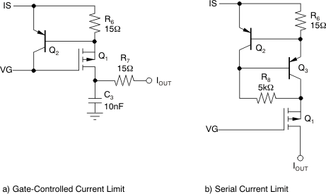
XTR111 External
                    Current Limit Circuits Figure 6-5 External Current Limit Circuits