SNAS333E August 2005 – December 2015 ADC128S052 , ADC128S052-Q1
PRODUCTION DATA.
The ADC128S052x device is a low-power, eight-channel CMOS 12-bit analog-to-digital converter specified for conversion throughput rates of
200 kSPS to 500 kSPS. The converter is based on a successive-approximation register architecture with an internal track-and-hold circuit. It can be configured to accept up to eight input signals at inputs IN0 through IN7.
The output serial data is straight binary and is compatible with several standards, such as SPI, QSPI, MICROWIRE, and many common DSP serial interfaces.
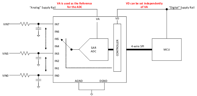
The ADC128S052x may be operated with independent analog and digital supplies. The analog supply (VA) can range from 2.7 V to 5.25 V, and the digital supply (VD) can range from 2.7 V to VA. Normal power consumption using a 3-V or
5-V supply is 1.6 mW and 8.7 mW, respectively. The power-down feature reduces the power consumption to 0.06 µW using a 3-V supply and 0.25 µW using a 5-V supply.
The ADC128S052x is packaged in a 16-pin TSSOP package. The ADC128S052 is ensured over the extended industrial temperature range of −40°C to +105°C while the ADC128S052-Q1 is ensured to an AECQ100 Grade-1 automotive temperature range of −40°C to +125°C.
PART NUMBER | PACKAGE | BODY SIZE (NOM) |
---|---|---|
ADC128S052, ADC128S052-Q1 |
TSSOP (16) | 4.40 mm × 5.00 mm |
Changes from D Revision (March 2013) to E Revision
Changes from C Revision (March 2013) to D Revision
PIN | TYPE | DESCRIPTION | |
---|---|---|---|
NO. | NAME | ||
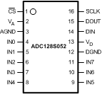
1 | CS | Digital I/O | Chip select. On the falling edge of CS, a conversion process begins. Conversions continue as long as CS is held low. |
2 | VA | Power Supply | Positive analog supply pin. This voltage is also used as the reference voltage. This pin must be connected to a quiet 2.7-V to 5.25-V source and bypassed to GND with 1-µF and 0.1-µF monolithic ceramic capacitors located within 1 cm of the power pin. |
3 | AGND | Power Supply | The ground return for the analog supply and signals. |
4 | IN0 to IN7 | Analog I/O | Analog inputs. These signals can range from 0 V to VREF. |
5 | |||
6 | |||
7 | |||
8 | |||
9 | |||
10 | |||
11 | |||
12 | DGND | Power Supply | The ground return for the digital supply and signals. |
13 | VD | Power Supply | Positive digital supply pin. This pin must be connected to a 2.7-V to VA supply, and bypassed to GND with a 0.1-µF monolithic ceramic capacitor located within 1 cm of the power pin. |
14 | DIN | Digital I/O | Digital data input. The control register of the ADC128S052 is loaded through this pin on rising edges of the SCLK pin. |
15 | DOUT | Digital I/O | Digital data output. The output samples are clocked out of this pin on the falling edges of the SCLK pin. |
16 | SCLK | Digital I/O | Digital clock input. The ensured performance range of frequencies for this input is 3.2 MHz to 8 MHz. This clock directly controls the conversion and readout processes. |
MIN | MAX | UNIT | ||
---|---|---|---|---|
Analog Supply Voltage VA | –0.3 | 6.5 | V | |
Digital Supply Voltage VD | –0.3 | VA + 0.3, max 6.5 | V | |
Voltage on Any Pin to GND | –0.3 | VA + 0.3 | V | |
Input Current at Any Pin(4) | ±10 | mA | ||
Package Input Current(4) | ±20 | mA | ||
Power Dissipation at TA = 25°C | See (5) | |||
Junction Temperature | +150 | °C | ||
Storage Temperature, Tstg | −65 | 150 | °C |
VALUE | UNIT | |||
---|---|---|---|---|
V(ESD) | Electrostatic discharge | Human body model (HBM), per ANSI/ESDA/JEDEC JS-001(1)(2) | ±2500 | V |
Machine model (MM)(3) | ±250 |
VALUE | UNIT | |||
---|---|---|---|---|
V(ESD) | Electrostatic discharge | Human-body model (HBM), per AEC Q100-002(1) | ±2500 | V |
Charged-device model (CDM), per AEC Q100-011 | ±250 |
MIN | NOM | MAX | UNIT | ||
---|---|---|---|---|---|
Operating Temperature | ADC128S052 | −40 | TA | 105 | °C |
ADC128S052-Q1 | −40 | TA | 125 | °C | |
VA Supply Voltage | 2.7 | 5.25 | V | ||
VD Supply Voltage | 2.7 | VA | V | ||
Digital Input Voltage | 0 | VA | V | ||
Analog Input Voltage | 0 | VA | V | ||
Clock Frequency | 50 | 1600 | kHz |
THERMAL METRIC(1) | ADC128S052, ADC128S052-Q1 | UNIT | |
---|---|---|---|
PW (TSSOP) | |||
16 PINS | |||
RθJA | Junction-to-ambient thermal resistance | 110 | °C/W |
RθJC(top) | Junction-to-case (top) thermal resistance | 42 | °C/W |
RθJB | Junction-to-board thermal resistance | 56 | °C/W |
ψJT | Junction-to-top characterization parameter | 5 | °C/W |
ψJB | Junction-to-board characterization parameter | 55 | °C/W |
PARAMETER | TEST CONDITIONS | MIN | TYP | MAX(1) | UNIT | |
---|---|---|---|---|---|---|
STATIC CONVERTER CHARACTERISTICS | ||||||
Resolution with No Missing Codes | 12 | Bits | ||||
INL | Integral Non-Linearity (End Point Method) | VA = VD = 3 V | ±0.3 | ±1 | LSB | |
VA = VD = 5 V | ±0.4 | ±1 | LSB | |||
DNL | Differential Non-Linearity | VA = VD = 3 V | 0.3 | 0.9 | LSB | |
−0.7 | −0.2 | LSB | ||||
VA = VD = 5 V | 0.6 | 1.3 | LSB | |||
−0.9 | −0.4 | LSB | ||||
VOFF | Offset Error | VA = VD = 3 V | 0.8 | ±2.3 | LSB | |
VA = VD = 5 V | 1.2 | ±2.3 | LSB | |||
OEM | Offset Error Match | VA = VD = 3 V | ±0.05 | ±1.5 | LSB | |
VA = VD = 5 V | ±0.2 | ±1.5 | LSB | |||
FSE | Full Scale Error | VA = VD = 3 V | 0.6 | ±2.0 | LSB | |
VA = VD = 5 V | 0.3 | ±2.0 | LSB | |||
FSEM | Full Scale Error Match | VA = VD = 3 V | ±0.05 | ±1.5 | LSB | |
VA = VD = 5 V | ±0.2 | ±1.5 | LSB | |||
DYNAMIC CONVERTER CHARACTERISTICS | ||||||
FPBW | Full Power Bandwidth (−3 dB) | VA = VD = 3 V | 8 | MHz | ||
VA = VD = 5 V | 11 | MHz | ||||
SINAD | Signal-to-Noise Plus Distortion Ratio | VA = VD = 3 V, fIN = 40.2 kHz, −0.02 dBFS |
70 | 73 | dB | |
VA = VD = 5 V, fIN = 40.2 kHz, −0.02 dBFS |
70 | 73 | dB | |||
SNR | Signal-to-Noise Ratio | VA = VD = 3 V, fIN = 40.2 kHz, −0.02 dBFS |
70.8 | 73 | dB | |
VA = VD = 5 V, fIN = 40.2 kHz, −0.02 dBFS |
70.8 | 73 | dB | |||
THD | Total Harmonic Distortion | VA = VD = 3 V, fIN = 40.2 kHz, −0.02 dBFS |
−90 | −74 | dB | |
VA = VD = 5 V, fIN = 40.2 kHz, −0.02 dBFS |
−89 | −74 | dB | |||
SFDR | Spurious-Free Dynamic Range | VA = VD = 3 V, fIN = 40.2 kHz, −0.02 dBFS |
75 | 92 | dB | |
VA = VD = 5 V, fIN = 40.2 kHz, −0.02 dBFS |
75 | 91 | dB | |||
ENOB | Effective Number of Bits | VA = VD = 3 V, fIN = 40.2 kHz |
11.3 | 11.8 | Bits | |
VA = VD = 5 V, fIN = 40.2 kHz, −0.02 dBFS |
11.3 | 11.8 | Bits | |||
ISO | Channel-to-Channel Isolation | VA = VD = 3 V, fIN = 20 kHz |
81 | dB | ||
VA = VD = 5 V, fIN = 20 kHz, −0.02 dBFS |
81 | dB | ||||
IMD | Intermodulation Distortion, Second Order Terms | VA = VD = 3 V, fa = 19.5 kHz, fb = 20.5 kHz |
−98 | dB | ||
VA = VD = 5 V, fa = 19.5 kHz, fb = 20.5 kHz |
−91 | dB | ||||
Intermodulation Distortion, Third Order Terms | VA = VD = 3 V, fa = 19.5 kHz, fb = 20.5 kHz |
−89 | dB | |||
VA = VD = 5 V, fa = 19.5 kHz, fb = 20.5 kHz |
−88 | dB | ||||
ANALOG INPUT CHARACTERISTICS | ||||||
VIN | Input Range | 0 | VA | V | ||
IDCL | DC Leakage Current | ±1 | µA | |||
CINA | Input Capacitance | Track Mode | 33 | pF | ||
Hold Mode | 3 | pF | ||||
DIGITAL INPUT CHARACTERISTICS | ||||||
VIH | Input High Voltage | VA = VD = 2.7 V to 3.6 V | 2.1 | V | ||
VA = VD = 4.75 V to 5.25 V | 2.4 | V | ||||
VIL | Input Low Voltage | VA = VD = 2.7 V to 5.25 V | 0.8 | V | ||
IIN | Input Current | VIN = 0 V or VD | ±0.01 | ±1 | µA | |
CIND | Digital Input Capacitance | 2 | 4 | pF | ||
DIGITAL OUTPUT CHARACTERISTICS | ||||||
VOH | Output High Voltage | ISOURCE = 200 µA, VA = VD = 2.7 V to 5.25 V |
VD − 0.5 | V | ||
VOL | Output Low Voltage | ISINK = 200 µA to 1.0 mA, VA = VD = 2.7 V to 5.25 V |
0.4 | V | ||
IOZH, IOZL | Hi-Impedance Output Leakage Current | VA = VD = 2.7 V to 5.25 V | ±1 | µA | ||
COUT | Hi-Impedance Output Capacitance(2) | 2 | 4 | pF | ||
Output Coding | Straight (Natural) Binary | |||||
POWER SUPPLY CHARACTERISTICS (CL = 10 pF) | ||||||
VA, VD | Analog and Digital Supply Voltages | VA ≥ VD | 2.7 | 5.25 | V | |
IA + ID | Total Supply Current Normal Mode ( CS low) |
VA = VD = 2.7 V to 3.6 V, fSAMPLE = 500 kSPS, fIN = 40 kHz |
0.54 | 1.2 | mA | |
VA = VD = 4.75 V to 5.25 V, fSAMPLE = 500 kSPS, fIN = 40 kHz |
1.74 | 2.6 | mA | |||
Total Supply Current Shutdown Mode (CS high) |
VA = VD = 2.7 V to 3.6 V, fSCLK = 0 kSPS |
20 | nA | |||
VA = VD = 4.75 V to 5.25 V, fSCLK = 0 kSPS |
50 | nA | ||||
PC | Power Consumption Normal Mode ( CS low) |
VA = VD = 3 V fSAMPLE = 500 kSPS, fIN = 40 kHz |
1.6 | 3.6 | mW | |
VA = VD = 5.0 V fSAMPLE = 500 kSPS, fIN = 40 kHz |
8.7 | 13.0 | mW | |||
Power Consumption Shutdown Mode (CS high) |
VA = VD = 3 V fSCLK = 0 kSPS |
0.06 | µW | |||
VA = VD = 5 V fSCLK = 0 kSPS |
0.25 | µW | ||||
AC ELECTRICAL CHARACTERISTICS | ||||||
fSCLKMIN | Minimum Clock Frequency | VA = VD = 2.7 V to 5.25 V | 3.2 | 0.8 | MHz | |
fSCLK | Maximum Clock Frequency | VA = VD = 2.7 V to 5.25 V | 16 | 8 | MHz | |
fS | Sample Rate Continuous Mode |
VA = VD = 2.7 V to 5.25 V | 200 | 50 | kSPS | |
1000 | 500 | kSPS | ||||
tCONVERT | Conversion (Hold) Time | VA = VD = 2.7 V to 5.25 V | 13 | SCLK cycles | ||
DC | SCLK Duty Cycle | VA = VD = 2.7 V to 5.25 V | 40% | 30% | ||
70% | 60% | |||||
tACQ | Acquisition (Track) Time | VA = VD = 2.7 V to 5.25 V | 3 | SCLK cycles | ||
Throughput Time | Acquisition Time + Conversion Time VA = VD = 2.7 V to 5.25 V |
16 | SCLK cycles | |||
tAD | Aperture Delay | VA = VD = 2.7 V to 5.25 V | 4 | ns |
MIN | NOM | MAX(1) | UNIT | |||
---|---|---|---|---|---|---|
tCSH | CS Hold Time after SCLK Rising Edge | 10 | 0 | ns | ||
tCSS | CS Set-up Time prior to SCLK Rising Edge | 10 | 4.5 | ns | ||
tEN | CS Falling Edge to DOUT enabled | 5 | 30 | ns | ||
tDACC | DOUT Access Time after SCLK Falling Edge | 17 | 27 | ns | ||
tDHLD | DOUT Hold Time after SCLK Falling Edge | 4 | ns | |||
tDS | DIN Set-up Time prior to SCLK Rising Edge | 10 | 3 | ns | ||
tDH | DIN Hold Time after SCLK Rising Edge | 10 | 3 | ns | ||
tCH | SCLK High Time | 0.4 × tSCLK | ns | |||
tCL | SCLK Low Time | 0.4 × tSCLK | ns | |||
tDIS | CS Rising Edge to DOUT High-Impedance | DOUT falling | 2.4 | 20 | ns | |
DOUT rising | 0.9 | 20 | ns |
VA = 5 V |
VA = 5 V |