-
AMC1304x-Q1 High-Precision, Reinforced Isolated Delta-Sigma Modulators with LDO SBAS799 February 2017 AMC1304L05-Q1 , AMC1304L25-Q1 , AMC1304M05-Q1 , AMC1304M25-Q1
PRODUCTION DATA.
-
AMC1304x-Q1 High-Precision, Reinforced Isolated Delta-Sigma Modulators with LDO
- 1 Features
- 2 Applications
- 3 Description
- 4 Revision History
- 5 Device Comparison Table
- 6 Pin Configurations and Functions
-
7 Specifications
- 7.1 Absolute Maximum Ratings
- 7.2 ESD Ratings
- 7.3 Recommended Operating Conditions
- 7.4 Thermal Information
- 7.5 Power Ratings
- 7.6 Insulation Specifications
- 7.7 Safety-Related Certifications
- 7.8 Safety Limiting Values
- 7.9 Electrical Characteristics: AMC1304x05-Q1
- 7.10 Electrical Characteristics: AMC1304x25-Q1
- 7.11 Switching Characteristics
- 7.12 Insulation Characteristics Curves
- 7.13 Typical Characteristics
- 8 Detailed Description
- 9 Application and Implementation
- 10Power-Supply Recommendations
- 11Layout
- 12Device and Documentation Support
- 13Mechanical, Packaging, and Orderable Information
- IMPORTANT NOTICE
パッケージ・オプション
メカニカル・データ(パッケージ|ピン)
- DW|16
サーマルパッド・メカニカル・データ
- DW|16
発注情報
AMC1304x-Q1 High-Precision, Reinforced Isolated Delta-Sigma Modulators with LDO
1 Features
- Qualified for Automotive Applications
- AEC-Q100 Qualified with the Following Results:
- Temperature Grade 1: –40°C to +125°C
- HBM ESD Classification Level 2
- CDM ESD Classification Level C6
-
Pin-Compatible Family with:
- ±50-mV or ±250-mV Input Voltage Ranges
- CMOS or LVDS Digital Interface Options
-
Excellent DC Performance:
- Offset Error: ±50 µV or ±100 µV (max)
- Offset Drift: 1.3 µV/°C (max)
- Gain Error: ±0.2% or ±0.3% (max)
- Gain Drift: ±40 ppm/°C (max)
- Safety-Related Certifications:
- 7000-VPK Reinforced Isolation per DIN V VDE V 0884-10 (VDE V 0884-10): 2006-12
- 5000-VRMS Isolation for 1 Minute per UL1577
- CAN/CSA No. 5A-Component Acceptance Service Notice
- Transient Immunity: 15 kV/µs (min)
- High Electromagnetic Field Immunity
(see Application Note SLLA181A) - External 5-MHz to 20-MHz Clock Input
- On-Chip 18-V LDO Regulator
2 Applications
- Shunt-Based Current Sensing or Resistor-Divider-Based Voltage Sensing In:
- Traction Inverters
- Onboard Chargers (OBC)
- DC-DC Converters
- Battery Management Systems (BMS)
3 Description
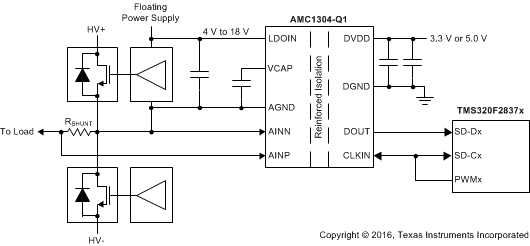
The AMC1304-Q1 is a precision, delta-sigma (ΔΣ) modulator with the output separated from the input circuitry by a capacitive double isolation barrier that is highly resistant to magnetic interference. This barrier is certified to provide reinforced isolation of up to 7000 VPEAK according to the DIN V VDE V 0884-10, UL1577 and CSA standards. Used in conjunction with isolated power supplies, the device prevents noise currents on a high common-mode voltage line from entering the local system ground and interfering with or damaging low voltage circuitry.
The input of the AMC1304-Q1 is optimized for direct connection to shunt resistors or other low voltage-level signal sources. The unique low input voltage range of the ±50-mV device allows significant reduction of the power dissipation through the shunt while supporting excellent ac and dc performance. By using an appropriate digital filter (that is, as integrated on the TMS320F2807x or TMS320F2837x families) to decimate the bit stream, the device can achieve 16 bits of resolution with a dynamic range of 81 dB (13.2 ENOB) at a data rate of 78 kSPS.
On the high-side, the modulator is supplied by an integrated low-dropout (LDO) regulator that allows an unregulated input voltage between 4 V and 18 V (LDOIN). The isolated digital interface operates from a 3.3-V or 5-V power supply (DVDD).
The AMC1304-Q1 is available in a wide-body SOIC-16 (DW) package.
Device Information(1)
| PART NUMBER | PACKAGE | BODY SIZE (NOM) |
|---|---|---|
| AMC1304x-Q1 | SOIC (16) | 10.30 mm × 7.50 mm |
- For all available packages, see the orderable addendum at the end of the datasheet.
Simplified Schematic
4 Revision History
| DATE | REVISION | NOTES |
|---|---|---|
| February 2017 | * | Initial release. |
5 Device Comparison Table
| DEVICE | INPUT VOLTAGE RANGE | DIFFERENTIAL INPUT RESISTANCE | DIGITAL OUTPUT INTERFACE |
|---|---|---|---|
| AMC1304L05-Q1 | ±50 mV | 5 kΩ | LVDS |
| AMC1304L25-Q1 | ±250 mV | 25 kΩ | LVDS |
| AMC1304M05-Q1 | ±50 mV | 5 kΩ | CMOS |
| AMC1304M25-Q1 | ±250 mV | 25 kΩ | CMOS |
6 Pin Configurations and Functions


Pin Functions
| PIN | I/O | DESCRIPTION | ||
|---|---|---|---|---|
| NAME | NO. | |||
| AMC1304Lx-Q1 (LVDS) |
AMC1304Mx-Q1 (CMOS) |
|||
| AGND | 4 | 4 | — | This pin is internally connected to pin 8 and can be left unconnected or tied to high-side ground |
| 8 | 8 | — | High-side ground reference | |
| AINN | 3 | 3 | I | Inverting analog input |
| AINP | 2 | 2 | I | Noninverting analog input |
| CLKIN | 13 | 13 | I | Modulator clock input, 5 MHz to 20.1 MHz |
| CLKIN_N | 12 | — | I | Inverted modulator clock input |
| DGND | 9, 16 | 9, 16 | — | Controller-side ground reference |
| DOUT | 11 | 11 | O | Modulator data output |
| DOUT_N | 10 | — | O | Inverted modulator data output |
| DVDD | 14 | 14 | — | Controller-side power supply, 3.0 V to 5.5 V. See the Power-Supply Recommendations section for decoupling recommendations. |
| LDOIN | 6 | 6 | — | Low dropout regulator input, 4 V to 18 V |
| NC | 1 | 1 | — | This pin can be connected to VCAP or left unconnected |
| 5 | 5 | — | This pin can be left unconnected or tied to AGND only | |
| — | 10, 12 | — | These pins have no internal connection | |
| 15 | 15 | — | This pin can be left unconnected or tied to DVDD only | |
| VCAP | 7 | 7 | — | LDO output. See the Power-Supply Recommendations section for decoupling recommendations. |
7 Specifications
7.1 Absolute Maximum Ratings
over the operating ambient temperature range (unless otherwise noted)(1)| MIN | MAX | UNIT | ||
|---|---|---|---|---|
| Supply voltage | DVDD to DGND | –0.3 | 6.5 | V |
| LDO input voltage | LDOIN to AGND | –0.3 | 26 | V |
| Analog input voltage at AINP, AINN | AGND – 6 | 3.7 | V | |
| Digital input voltage at CLKIN, CLKIN_N | DGND – 0.3 | DVDD + 0.3 | V | |
| Input current to any pin except supply pins | –10 | 10 | mA | |
| Junction temperature, TJ | 150 | °C | ||
| Storage temperature, Tstg | –65 | 150 | °C | |
7.2 ESD Ratings
| VALUE | UNIT | |||
|---|---|---|---|---|
| V(ESD) | Electrostatic discharge | Human body model (HBM), per AEC Q100-002(1) | ±2500 | V |
| Charged device model (CDM), per AEC Q100-011 | ±1000 | |||
7.3 Recommended Operating Conditions
over operating free-air temperature range (unless otherwise noted)| MIN | NOM | MAX | UNIT | ||
|---|---|---|---|---|---|
| LDOIN | LDO input supply voltage (LDOIN pin) | 4.0 | 15.0 | 18.0 | V |
| DVDD | Digital (controller-side) supply voltage (DVDD pin) | 3.0 | 3.3 | 5.5 | V |
| TA | Operating ambient temperature range | –40 | 125 | °C | |
7.4 Thermal Information
| THERMAL METRIC (1) | AMC1304x-Q1 | UNIT | |
|---|---|---|---|
| DW (SOIC) | |||
| 16 PINS | |||
| RθJA | Junction-to-ambient thermal resistance | 80.2 | °C/W |
| RθJC(top) | Junction-to-case (top) thermal resistance | 40.5 | °C/W |
| RθJB | Junction-to-board thermal resistance | 45.1 | °C/W |
| ψJT | Junction-to-top characterization parameter | 11.9 | °C/W |
| ψJB | Junction-to-board characterization parameter | 44.5 | °C/W |
| RθJC(bot) | Junction-to-case (bottom) thermal resistance | n/a | °C/W |
7.5 Power Ratings
| PARAMETER | TEST CONDITIONS | VALUE | UNIT | |
|---|---|---|---|---|
| PD | Maximum power dissipation (both sides) | LDOIN = 18 V, DVDD = 5.5 V | 161 | mW |
| PD1 | Maximum power dissipation (high-side supply) | LDOIN = 18 V | 117 | mW |
| PD2 | Maximum power dissipation (low-side supply) | DVDD = 5.5 V, LVDS, RLOAD = 100 Ω | 44 | mW |
7.6 Insulation Specifications
| PARAMETER | TEST CONDITIONS | VALUE | UNIT | |
|---|---|---|---|---|
| GENERAL | ||||
| CLR | Minimum air gap (clearance)(1) | Shortest pin-to-pin distance through air | ≥ 8 | mm |
| CPG | Minimum external tracking (creepage)(1) | Shortest pin-to-pin distance across the package surface | ≥ 8 | mm |
| DTI | Distance through insulation | Minimum internal gap (internal clearance) of the double insulation (2 × 0.0135 mm) | 0.027 | mm |
| CTI | Comparative tracking index | DIN EN 60112 (VDE 0303-11); IEC 60112 | ≥ 600 | V |
| Material group | According to IEC 60664-1 | I | ||
| Overvoltage category per IEC 60664-1 | Rated mains voltage ≤ 300 VRMS | I-IV | ||
| Rated mains voltage ≤ 600 VRMS | I-III | |||
| Rated mains voltage ≤ 1000 VRMS | I-II | |||
| DIN V VDE V 0884-10 (VDE V 0884-10): 2006-12(2) | ||||
| VIORM | Maximum repetitive peak isolation voltage | At ac voltage (bipolar or unipolar) | 1414 | VPK |
| VIOWM | Maximum-rated isolation working voltage | At ac voltage (sine wave) | 1000 | VRMS |
| At dc voltage | 1500 | VDC | ||
| VIOTM | Maximum transient isolation voltage | VTEST = VIOTM, t = 60 s (qualification test) | 7000 | VPK |
| VTEST = 1.2 x VIOTM, t = 1 s (100% production test) | 8400 | |||
| VIOSM | Maximum surge isolation voltage(3) | Test method per IEC 60065, 1.2/50-μs waveform, VTEST = 1.6 x VIOSM = 10000 VPK (qualification) | 6250 | VPK |
| qpd | Apparent charge(4) | Method a, after input/output safety test subgroup 2 / 3, Vini = VIOTM, tini = 60 s, Vpd(m) = 1.2 x VIORM = 1697 VPK, tm = 10 s | ≤ 5 | pC |
| Method a, after environmental tests subgroup 1, Vini = VIOTM, tini = 60 s, Vpd(m) = 1.6 x VIORM = 2263 VPK, tm = 10 s | ≤ 5 | pC | ||
| Method b1, at routine test (100% production) and preconditioning (type test), Vini = VIOTM, tini = 1 s, Vpd(m) = 1.875 x VIORM = 2652 VPK, tm = 1 s | ≤ 5 | pC | ||
| CIO | Barrier capacitance, input to output(5) | VIO = 0.5 VPP at 1 MHz | 1.2 | pF |
| RIO | Insulation resistance, input to output(5) | VIO = 500 V at TS = 150°C | > 109 | Ω |
| Pollution degree | 2 | |||
| Climatic category | 40/125/21 | |||
| UL1577 | ||||
| VISO | Withstand isolation voltage | VTEST = VISO = 5000 VRMS or 7000 VDC, t = 60 s (qualification test), VTEST = 1.2 x VISO = 6000 VRMS, t = 1 s (100% production test) | 5000 | VRMS |
7.7 Safety-Related Certifications
| VDE | UL | ||
|---|---|---|---|
| Certified according to DIN V VDE V 0884-10 (VDE V 0884-10): 2006-12, DIN EN 60950-1 (VDE 0805 Teil 1): 2014-08, and DIN EN 60095 (VDE 0860): 2005-11 | Recognized under UL1577 component recognition and CSA component acceptance NO 5 programs | ||
| Reinforced insulation | Single protection | ||
| File number: 40040142 | File number: E181974 |
7.8 Safety Limiting Values
Safety limiting intends to prevent potential damage to the isolation barrier upon failure of input or output (I/O) circuitry. A failure of the I/O circuitry may allow low resistance to ground or the supply and, without current limiting, dissipate sufficient power to overheat the die and damage the isolation barrier, potentially leading to secondary system failures.| PARAMETER | TEST CONDITIONS | MIN | TYP | MAX | UNIT | |
|---|---|---|---|---|---|---|
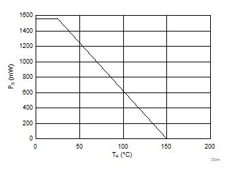
| IS | Safety input, output, or supply current | θJA = 80.2°C/W, LDOIN = 18 V, TJ = 150°C, TA = 25°C, see Figure 3 |
86.5 | mA | ||
| PS | Safety input, output, or total power | θJA = 80.2°C/W, TJ = 150°C, TA = 25°C, see Figure 4 | 1558(1) | mW | ||
| TS | Maximum safety temperature | 150 | °C | |||
The maximum safety temperature is the maximum junction temperature specified for the device. The power dissipation and junction-to-air thermal impedance of the device installed in the application hardware determines the junction temperature. The assumed junction-to-air thermal resistance in the Thermal Information table is that of a device installed on a high-K test board for leaded surface-mount packages. The power is the recommended maximum input voltage times the current. The junction temperature is then the ambient temperature plus the power times the junction-to-air thermal resistance.
7.9 Electrical Characteristics: AMC1304x05-Q1
All minimum and maximum specifications are at TA = –40°C to 125°C, LDOIN = 4.0 V to 18.0 V, DVDD = 3.0 V to 5.5 V, AINP = –50 mV to 50 mV, AINN = 0 V, and sinc3 filter with OSR = 256, unless otherwise noted. Typical values are at TA = 25°C, CLKIN = 20 MHz, LDOIN = 15.0 V, and DVDD = 3.3 V.| PARAMETER | TEST CONDITIONS | MIN | TYP | MAX | UNIT | |
|---|---|---|---|---|---|---|
| ANALOG INPUTS | ||||||
| VClipping | Maximum differential voltage input range (AINP-AINN) |
±62.5 | mV | |||
| FSR | Specified linear full-scale range (AINP-AINN) |
–50 | 50 | mV | ||
| VCM | Operating common-mode input range | –0.032 | 1.2 | V | ||
| CID | Differential input capacitance | 2 | pF | |||
| IIB | Input bias current | Inputs shorted to AGND | –97 | –72 | –57 | μA |
| RID | Differential input resistance | 5 | kΩ | |||
| IIO | Input offset current | ±5 | nA | |||
| CMTI | Common-mode transient immunity | 15 | kV/μs | |||
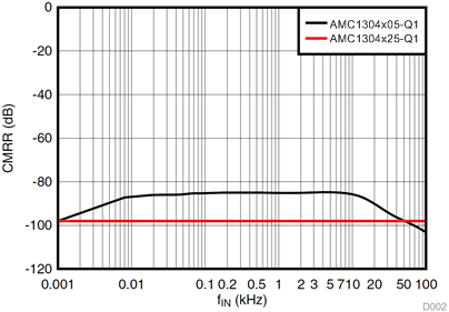
| CMRR | Common-mode rejection ratio | fIN = 0 Hz, VCM min ≤ VIN ≤ VCM max |
–98 | dB | ||
| fIN from 0.1 Hz to 50 kHz, VCM min ≤ VIN ≤ VCM max |
–85 | |||||
| BW | Input bandwidth | 800 | kHz | |||
| DC ACCURACY | ||||||
| DNL | Differential nonlinearity | Resolution: 16 bits | –0.99 | 0.99 | LSB | |
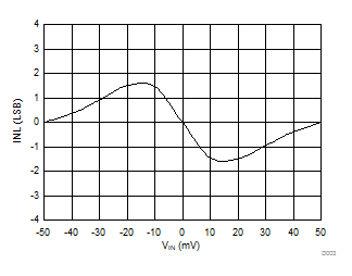
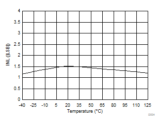
| INL | Integral nonlinearity (1) | Resolution: 16 bits | –5 | ±1.5 | 5 | LSB |
| EO | Offset error | Initial, at 25°C | –50 | ±2.5 | 50 | µV |
| TCEO | Offset error thermal drift (2) | –1.3 | 1.3 | μV/°C | ||
| EG | Gain error | Initial, at 25°C | –0.3% | –0.02% | 0.3% | |
| TCEG | Gain error thermal drift (3) | –40 | ±20 | 40 | ppm/°C | |
| PSRR | Power-supply rejection ratio | LDOIN from 4 V to 18 V, at dc | –110 | dB | ||
| LDOIN from 4 V to 18 V, from 0.1 Hz to 50 kHz | –110 | |||||
| AC ACCURACY | ||||||
| SNR | Signal-to-noise ratio | fIN = 1 kHz | 76 | 81.5 | dB | |
| SINAD | Signal-to-noise + distortion | fIN = 1 kHz | 76 | 81 | dB | |
| THD | Total harmonic distortion | fIN = 1 kHz | –90 | –81 | dB | |
| SFDR | Spurious-free dynamic range | fIN = 1 kHz | 81 | 90 | dB | |
| DIGITAL INPUTS/OUTPUTS | ||||||
| External Clock | ||||||
| fCLKIN | Input clock frequency | 5 | 20 | 20.1 | MHz | |
| DutyCLKIN | Duty cycle | 5 MHz ≤ fCLKIN ≤ 20.1 MHz | 40% | 50% | 60% | |
| CMOS Logic Family (AMC1304M05-Q1, CMOS with Schmitt Trigger) | ||||||
| IIN | Input current | DGND ≤ VIN ≤ DVDD | –1 | 1 | μA | |
| CIN | Input capacitance | 5 | pF | |||
| VIH | High-level input voltage | 0.7 × DVDD | DVDD + 0.3 | V | ||
| VIL | Low-level input voltage | –0.3 | 0.3 × DVDD | V | ||
| CLOAD | Output load capacitance | fCLKIN = 20 MHz | 30 | pF | ||
| VOH | High-level output voltage | IOH = –20 µA | DVDD – 0.1 | V | ||
| IOH = –4 mA | DVDD – 0.4 | |||||
| VOL | Low-level output voltage | IOL = 20 µA | 0.1 | V | ||
| IOL = 4 mA | 0.4 | |||||
| LVDS Logic Family (AMC1304L05-Q1)(4) | ||||||
| VT | Differential output voltage | RLOAD = 100 Ω | 250 | 350 | 450 | mV |
| VOC | Common-mode output voltage | 1.125 | 1.23 | 1.375 | V | |
| VID | Differential input voltage | 100 | 350 | 600 | mV | |
| VIC | Common-mode input voltage | VID = 100 mV | 0.05 | 1.25 | 3.25 | V |
| II | Receiver input current | DGND ≤ VIN ≤ 3.3 V | –24 | 0 | 20 | µA |
| POWER SUPPLY | ||||||
| LDOIN | LDOIN pin input voltage | 4.0 | 15.0 | 18.0 | V | |
| VCAP | VCAP pin voltage | 3.45 | V | |||
| ILDOIN | LDOIN pin input current | 5.3 | 6.5 | mA | ||
| DVDD | Controller-side supply voltage | 3.0 | 3.3 | 5.5 | V | |
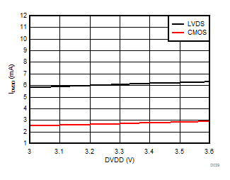
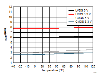
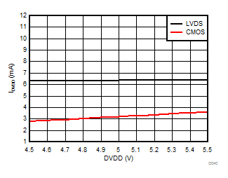
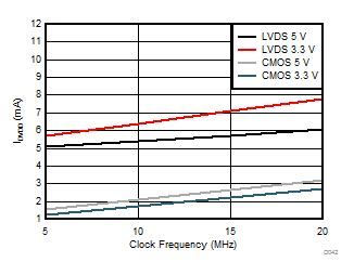
| IDVDD | Controller-side supply current | LVDS, RLOAD = 100 Ω | 6.1 | 8 | mA | |
| CMOS, 3.0 V ≤ DVDD ≤ 3.6 V, CLOAD = 5 pF |
2.7 | 4.0 | ||||
| CMOS, 4.5 V ≤ DVDD ≤ 5.5 V, CLOAD = 5 pF |
3.2 | 5.5 | ||||


7.10 Electrical Characteristics: AMC1304x25-Q1
All minimum and maximum specifications are at TA = –40°C to 125°C, LDOIN = 4.0 V to 18.0 V, DVDD = 3.0 V to 5.5 V, AINP = –250 mV to 250 mV, AINN = 0 V, and sinc3 filter with OSR = 256, unless otherwise noted. Typical values are at TA = 25°C, CLKIN = 20 MHz, LDOIN = 15.0 V, and DVDD = 3.3 V.| PARAMETER | TEST CONDITIONS | MIN | TYP | MAX | UNIT | |
|---|---|---|---|---|---|---|
| ANALOG INPUTS | ||||||
| VClipping | Maximum differential voltage input range (AINP-AINN) |
±312.5 | mV | |||
| FSR | Specified linear full-scale range (AINP-AINN) |
–250 | 250 | mV | ||
| VCM | Operating common-mode input range | –0.16 | 1.2 | V | ||
| CID | Differential input capacitance | 1 | pF | |||
| IIB | Input bias current | Inputs shorted to AGND | –82 | –60 | –48 | μA |
| RID | Differential input resistance | 25 | kΩ | |||
| IIO | Input offset current | ±5 | nA | |||
| CMTI | Common-mode transient immunity | 15 | kV/μs | |||
| CMRR | Common-mode rejection ratio | fIN = 0 Hz, VCM min ≤ VIN ≤ VCM max |
–98 | dB | ||
| fIN from 0.1 Hz to 50 kHz, VCM min ≤ VIN ≤ VCM max |
–98 | |||||
| BW | Input bandwidth | 1000 | kHz | |||
| DC ACCURACY | ||||||
| DNL | Differential nonlinearity | Resolution: 16 bits | –0.99 | 0.99 | LSB | |
| INL | Integral nonlinearity(1) | Resolution: 16 bits | –4 | ±1.5 | 4 | LSB |
| EO | Offset error | Initial, at 25°C | –100 | ±25 | 100 | µV |
| TCEO | Offset error thermal drift(2) | –1.3 | 1.3 | μV/°C | ||
| EG | Gain error | Initial, at 25°C | –0.2% | –0.05% | 0.2% | |
| TCEG | Gain error thermal drift(3) | –40 | ±20 | 40 | ppm/°C | |
| PSRR | Power-supply rejection ratio | LDOIN from 4 V to 18 V, at dc | –110 | dB | ||
| LDOIN from 4 V to 18 V, from 0.1 Hz to 50 kHz |
–110 | |||||
| AC ACCURACY | ||||||
| SNR | Signal-to-noise ratio | fIN = 1 kHz | 82 | 85 | dB | |
| SINAD | Signal-to-noise + distortion | fIN = 1 kHz | 80 | 84 | dB | |
| THD | Total harmonic distortion | fIN = 1 kHz | –90 | –81 | dB | |
| SFDR | Spurious-free dynamic range | fIN = 1 kHz | 81 | 90 | dB | |
| DIGITAL INPUTS/OUTPUTS | ||||||
| External Clock | ||||||
| fCLKIN | Input clock frequency | 5 | 20 | 20.1 | MHz | |
| DutyCLKIN | Duty cycle | 5 MHz ≤ fCLKIN ≤ 20.1 MHz | 40% | 50% | 60% | |
| CMOS Logic Family (AMC1304M25-Q1, CMOS with Schmitt Trigger) | ||||||
| IIN | Input current | DGND ≤ VIN ≤ DVDD | –1 | 1 | μA | |
| CIN | Input capacitance | 5 | pF | |||
| VIH | High-level input voltage | 0.7 × DVDD | DVDD + 0.3 | V | ||
| VIL | Low-level input voltage | –0.3 | 0.3 × DVDD | V | ||
| CLOAD | Output load capacitance | fCLKIN = 20 MHz | 30 | pF | ||
| VOH | High-level output voltage | IOH = –20 µA | DVDD – 0.1 | V | ||
| IOH = –4 mA | DVDD – 0.4 | V | ||||
| VOL | Low-level output voltage | IOL = 20 µA | 0.1 | V | ||
| IOL = 4 mA | 0.4 | V | ||||
| LVDS Logic Family (AMC1304L25-Q1)(4) | ||||||
| VT | Differential output voltage | RLOAD = 100 Ω | 250 | 350 | 450 | mV |
| VOC | Common-mode output voltage | 1.125 | 1.23 | 1.375 | V | |
| VID | Differential input voltage | 100 | 350 | 600 | mV | |
| VIC | Common-mode input voltage | VID = 100 mV | 0.05 | 1.25 | 3.25 | V |
| II | Receiver input current | DGND ≤ VIN ≤ 3.3 V | –24 | 0 | 20 | µA |
| POWER SUPPLY | ||||||
| LDOIN | LDOIN pin input voltage | 4.0 | 15.0 | 18.0 | V | |
| VCAP | VCAP pin voltage | 3.45 | V | |||
| ILDOIN | LDOIN pin input current | 5.3 | 6.5 | mA | ||
| DVDD | Controller-side supply voltage | 3.0 | 3.3 | 5.5 | V | |
| IDVDD | Controller-side supply current | LVDS, RLOAD = 100 Ω | 6.1 | 8.0 | mA | |
| CMOS, 3.0 V ≤ DVDD ≤ 3.6 V, CLOAD = 5 pF |
2.7 | 4.0 | ||||
| CMOS, 4.5 V ≤ DVDD ≤ 5.5 V, CLOAD = 5 pF |
3.2 | 5.5 | ||||
 .
.  .
.7.11 Switching Characteristics
over operating free-air temperature range (unless otherwise noted)| PARAMETER | TEST CONDITIONS | MIN | TYP | MAX | UNIT | |
|---|---|---|---|---|---|---|
| tCLK | CLKIN, CLKIN_N clock period | 49.75 | 50 | 200 | ns | |
| tHIGH | CLKIN, CLKIN_N clock high time | 19.9 | 25 | 120 | ns | |
| tLOW | CLKIN, CLKIN_N clock low time | 19.9 | 25 | 120 | ns | |
| tD | Falling edge of CLKIN, CLKIN_N to DOUT, DOUT_N valid delay | 0 | 15 | ns | ||
| tISTART | Interface startup time | DVDD at 3.0 V (min) to DOUT, DOUT_N valid with LDO_IN > 4 V | 32 | 32 | CLKIN cycles | |
| tASTART | Analog startup time | LDOIN step to 4 V with DVDD ≥ 3.0 V, and 0.1 µF at VCAP pin | 1 | ms | ||
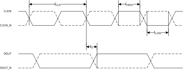 Figure 1. Digital Interface Timing
 Figure 2. Digital Interface Startup Timing
7.12 Insulation Characteristics Curves
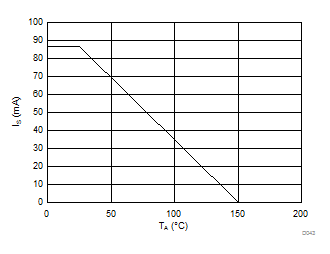
| LDOIN = 18 V (worst case) |
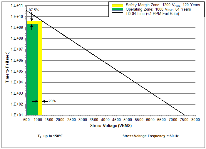
| TA up to 150°C, stress voltage frequency = 60 Hz |
7.13 Typical Characteristics
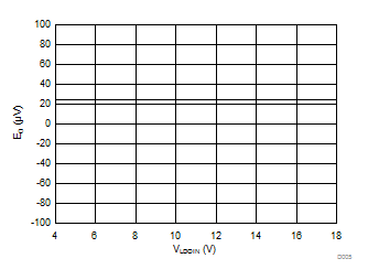
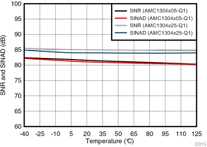
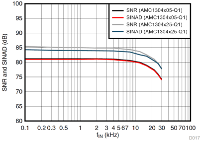
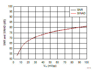
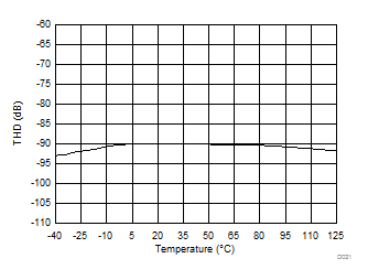
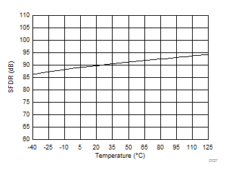
At LDOIN = 15.0 V, DVDD = 3.3 V, AINP = –50 mV to 50 mV (AMC1304x05-Q1) or –250 mV to 250 mV (AMC1304x25-Q1), AINN = 0 V, fCLKIN = 20 MHz, and sinc3 filter with OSR = 256, unless otherwise noted.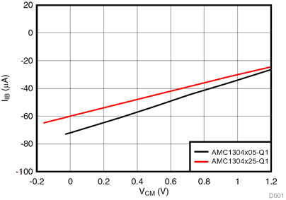
| AMC1304x25-Q1 |
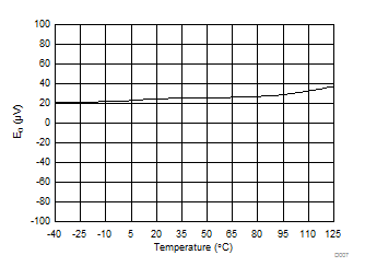
| AMC1304x25-Q1 |
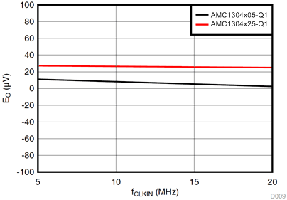
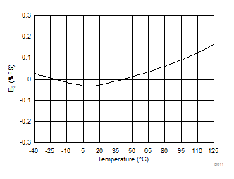
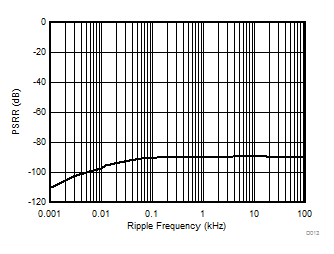
Ripple Frequency
| AMC1304x05-Q1 |
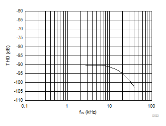
Input Signal Frequency
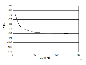
| AMC1304x05-Q1 |
Input Signal Amplitude
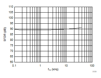
Input Signal Frequency
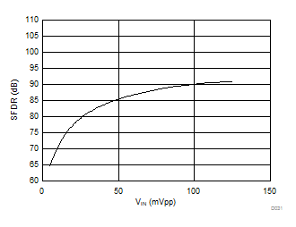
| AMC1304x05-Q1 |
Input Signal Amplitude
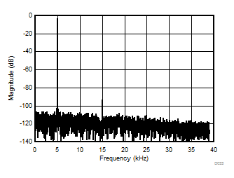
| AMC1304x05-Q1, 4096-point FFT, VIN = 100 mVPP |
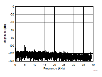
| AMC1304x25-Q1, 4096-point FFT, VIN = 500 mVPP |
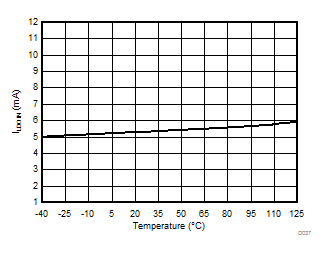
Controller-Side Supply Voltage (3.3 V, min)
Input Signal Frequency
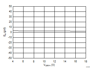
| AMC1304x05-Q1 |
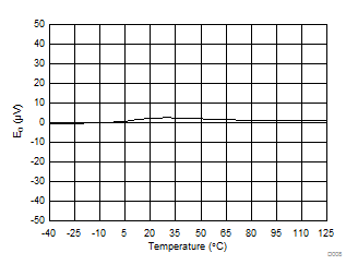
| AMC1304x05-Q1 |
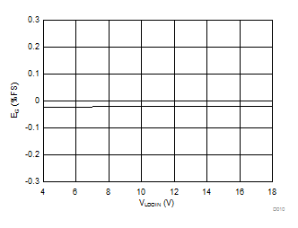
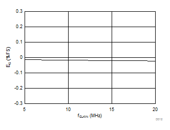
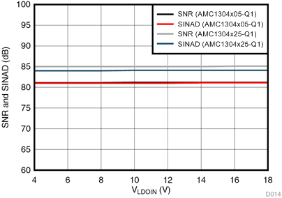
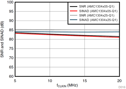
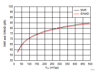
| AMC1304x25-Q1 |
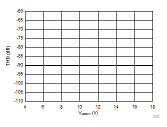
LDO Input Supply Voltage
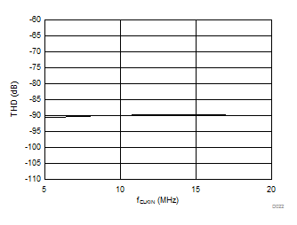
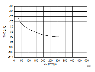
| AMC1304x25-Q1 |
Input Signal Amplitude
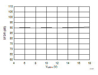
LDO Input Supply Voltage
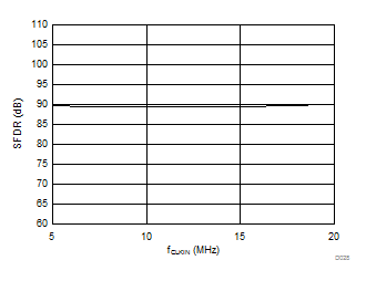
Clock Frequency
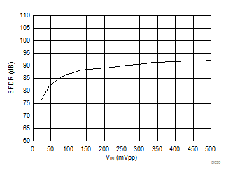
| AMC1304x25-Q1 |
Input Signal Amplitude
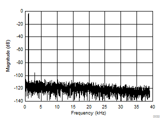
| AMC1304x05-Q1, 4096-point FFT, VIN = 100 mVPP |

| AMC1304x25-Q1, 4096-point FFT, VIN = 500 mVPP |
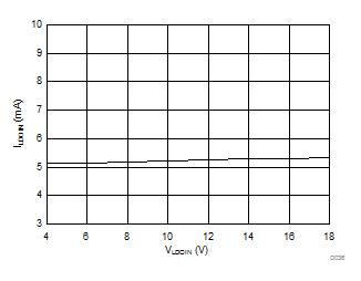
LDO Input Supply Voltage
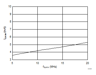
Controller-Side Supply Voltage (5 V, min)
Clock Frequency