SCAS847I July 2007 – October 2016 CDCE925 , CDCEL925
PRODUCTION DATA.
- 1 Features
- 2 Applications
- 3 Description
- 4 Revision History
- 5 Description (continued)
- 6 Pin Configuration and Functions
- 7 Specifications
- 8 Parameter Measurement Information
- 9 Detailed Description
- 10Application and Implementation
- 11Power Supply Recommendations
- 12Layout
- 13Device and Documentation Support
- 14Mechanical, Packaging, and Orderable Information
1 Features
- Member of Programmable Clock Generator Family
- CDCEx913: 1-PLL, 3 Outputs
- CDCEx925: 2-PLL, 5 Outputs
- CDCEx925: 3-PLL, 7 Outputs
- CDCEx949: 4-PLL, 9 Outputs
- In-System Programmability and EEPROM
- Serial Programmable Volatile Register
- Nonvolatile EEPROM to Store Customer Settings
- Flexible Input Clocking Concept
- External Crystal: 8 MHz to 32 MHz
- On-Chip VCXO: Pull Range ±150 ppm
- Single-Ended LVCMOS Up to 160 MHz
- Free Selectable Output Frequency Up to 230 MHz
- Low-Noise PLL Core
- PLL Loop Filter Components Integrated
- Low Period Jitter (Typical 60 ps)
- Separate Output Supply Pins
- CDCE925: 3.3 V and 2.5 V
- CDCEL925: 1.8 V
- Flexible Clock Driver
- Three User-Definable Control Inputs [S0/S1/S2], for Example, SSC Selection, Frequency Switching, Output Enable, or Power Down
- Generates Highly Accurate Clocks for Video, Audio, USB, IEEE1394, RFID, Bluetooth®, WLAN, Ethernet™, and GPS
- Generates Common Clock Frequencies Used With TI-DaVinci™, OMAP™, DSPs
- Programmable SSC Modulation
- Enables 0-PPM Clock Generation
- 1.8-V Device Power Supply
- Wide Temperature Range: –40°C to 85°C
- Packaged in TSSOP
- Development and Programming Kit for Easy PLL Design and Programming (TI Pro-Clock™)
2 Applications
D-TVs, STBs, IP-STBs, DVD Players, DVD Recorders, and Printers
3 Description
The CDCE925 and CDCEL925 are modular PLL-based low-cost, high-performance, programmable clock synthesizers, multipliers, and dividers. They generate up to five output clocks from a single input frequency. Each output can be programmed in-system for any clock frequency up to 230 MHz, using up to two independent configurable PLLs.
The CDCEx925 has a separate output supply pin, VDDOUT, which is 1.8 V for CDCEL925 and 2.5 V to 3.3 V for CDCE925.
The input accepts an external crystal or LVCMOS clock signal. In case of a crystal input, an on-chip load capacitor is adequate for most applications. The value of the load capacitor is programmable from 0 to 20 pF. Additionally, an on-chip VCXO is selectable which allows synchronization of the output frequency to an external control signal, that is, PWM signal.
Device Information(1)
| PART NUMBER | PACKAGE | BODY SIZE (NOM) |
|---|---|---|
| CDCEx925 | TSSOP (16) | 5.00 mm x 4.40 mm |
- For all available packages, see the orderable addendum at the end of the data sheet.
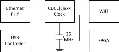
Typical Application Schematic

4 Revision History
Changes from H Revision (August 2016) to I Revision
- Changed data sheet title from: CDCEx925 Programmable 2-PLL VCXO Clock Synthesizer With 1.8-V, 2.5-V, 3.3-V LVCMOS Outputs to: CDCE(L)925: Flexible Low Power LVCMOS Clock Generator With SSC Support for EMI ReductionGo
Changes from G Revision (November 2011) to H Revision
- Added Device Information table, ESD Ratings table, Feature Description section, Device Functional Modes, Application and Implementation section, Power Supply Recommendations section, Layout section, Device and Documentation Support section, and Mechanical, Packaging, and Orderable Information sectionGo
- Changed RθJB from 64°C/W : to 63.63°C/WGo
- Changed ψJT from 1.0°C/W : to 1.01°C/WGo
- Added ψJB parameter to Thermal Information tableGo
- Deleted figureGo
Changes from F Revision (March 2010) to G Revision
- Changed in Figure 9, second S to SrGo
- Changed under second where page 21 from N′ = N × 2PN ≥ M100 MHz ≤ ƒVCO ≤ 200 MHz; TO 3 lines with last line being changed to 80 MHz ≤ ƒVCO ≤ 230 MHz and 0 ≤ p ≤ 7 changed to 0 ≤ p ≤ 4Go
Changes from E Revision (October 2009) to F Revision
- Added PLL settings limits: 16 ≤ q ≤ 63, 0 ≤ p ≤ 7, 0 ≤ r ≤ 511, 0 < N < 4096 to PLL1 and PLL2 Configure Register tablesGo
- Added PLL settings limits: 16 ≤ q ≤ 63, 0 ≤ p ≤ 7, 0 ≤ r ≤ 511, 0 < N < 511 to PLL Multiplier/Divder Definition SectionGo
Changes from D Revision (September 2009) to E Revision
- Deleted sentence - A different default setting can be programmed on customer request. Contact Texas Instruments sales or marketing representative for more information.Go
Changes from C Revision (December 2007) to D Revision
- Added Note 3: SDA and SCL can go up to 3.6 V as stated in the Recommended Operating Conditions tableGo
Changes from B Revision (August 2007) to C Revision
- Changed all values except in add rows: Original - 108, 102, 100, 96, 34Go
- Changed Generic Configuration Register table RID From: 0h To: XbGo
- Added note to the PWDN description in Generic Configuration Register tableGo
Changes from A Revision (August 2007) to B Revision
- Changed IDDPD Power-down current Typ value from 20 to 30Go
- Changed II LVCMOS Input current Typ value from ±5 to ±5 MaxGo
- Changed IIH LVCMOS Input current for S0/S1/S2 value from 5 Typ to 5 MaxGo
- Changed IIL LVCMOS Input current for S0/S1/S2 value from –4 Typ to –4 MaxGo
- Changed text of Note 4 in the DEVICE CHARACTERISTIC tableGo
- Changed Test Load for 50-Ω Board EnvironmentGo
- Changed PLL Setting table header From: OUTPUT SELECTION (Y2 ... Y9) To: OUTPUT SELECTION (Y2 ... Y5)Go
- Changed Generic Configuration Register table 01h Bit 7 From: For interla use – always write To: Reserved – always write Go
- Changed PLL2 Configuration Register table PLL2_1N [11:4] description From: fVCO1_1 To: fVCO2_1 Go
Changes from * Revision (July 2007) to A Revision
- Changed the data sheet status From: Product Preview To: Production dataGo