CSD22202W15 P-Channel NexFET Power MOSFET
1 Features
- Low Resistance
- Small Footprint 1.5 mm × 1.5 mm
- Pb Free
- Gate ESD Protection
- RoHS Compliant
- Halogen Free
- Gate-Source Voltage Clamp
2 Applications
- Battery Management
- Battery Protection
- Load Switch Applications
3 Description
The device is designed to deliver the lowest on resistance and gate charge in the smallest outline possible with excellent thermal characteristics in an ultra-low profile. Low on resistance coupled with the small footprint and low profile make the device ideal for battery operated space constrained applications.

Product Summary
Ordering Information(1)
| Device | Qty | Media | Package | Ship |
|---|---|---|---|---|
| CSD22202W15 | 3000 | 7-Inch Reel | 1.5 mm × 1.5 mm Wafer BGA Package | Tape and Reel |
| CSD22202W15T | 250 | 7-Inch Reel |
- For all available packages, see the orderable addendum at the end of the data sheet.
Absolute Maximum Ratings
| TA = 25°C unless otherwise stated | VALUE | UNIT | |
|---|---|---|---|
| VDS | Drain-to-Source Voltage | –8 | V |
| VGS | Gate-to-Source Voltage | –6 | V |
| ID | Continuous Drain Current(1)
(Silicon Limitted) |
–10 | A |
| Pulsed Drain Current(2) | –48 | ||
| IG | Continuous Gate Current(3) | –0.5 | A |
| PD | Power Dissipation(1) | 1.5 | W |
| TJ, Tstg |
Operating Junction and Storage Temperature Range |
–55 to 150 | °C |
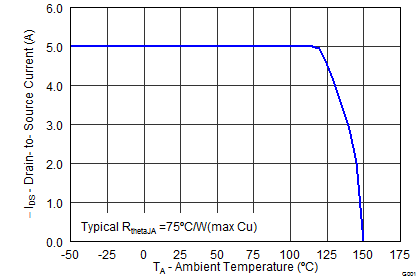
- RθJA = 75°C/W on 1in2 Cu (2 oz.) on 0.060" thick FR4 PCB.
- Pulse width ≤ 300 µs, duty cycle ≤ 2%
- Limited by gate resistance.
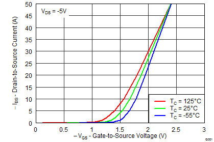
RDS(on) vs VGS |
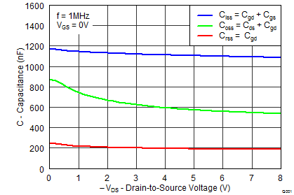
Gate Charge |
4 Revision History
Changes from A Revision (July 2014) to B Revision
- Corrected typo, test condition VDS is –6.4 V for IDDSGo
- Corrected typo, test condition VGS is –6 V for IGSSGo
Changes from * Revision (June 2013) to A Revision
- Corrected "Drain to Drain Voltage" to state "Drain-to-Source Voltage" Go
5 Specifications
5.1 Electrical Characteristics
(TA = 25°C unless otherwise stated)5.2 Thermal Information
(TA = 25°C unless otherwise stated)| THERMAL METRIC | TYPICAL VALUES | UNIT | |||
|---|---|---|---|---|---|
| RθJA | Junction-to-Ambient Thermal Resistance(1) | 75 | °C/W | ||
| Junction-to-Ambient Thermal Resistance(2) | 210 | ||||
 |
Typ RθJA = 75°C/W when mounted on 1inch2 of 2 oz. Cu. |
 |
Typ RθJA = 210°C/W when mounted on minimum pad area of 2 oz. Cu. |
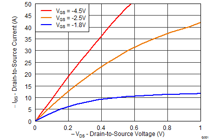
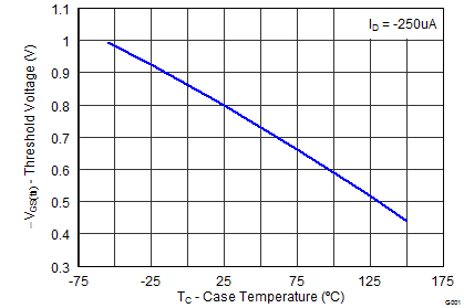
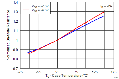
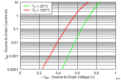
5.3 Typical MOSFET Characteristics
(TA = 25°C unless otherwise stated)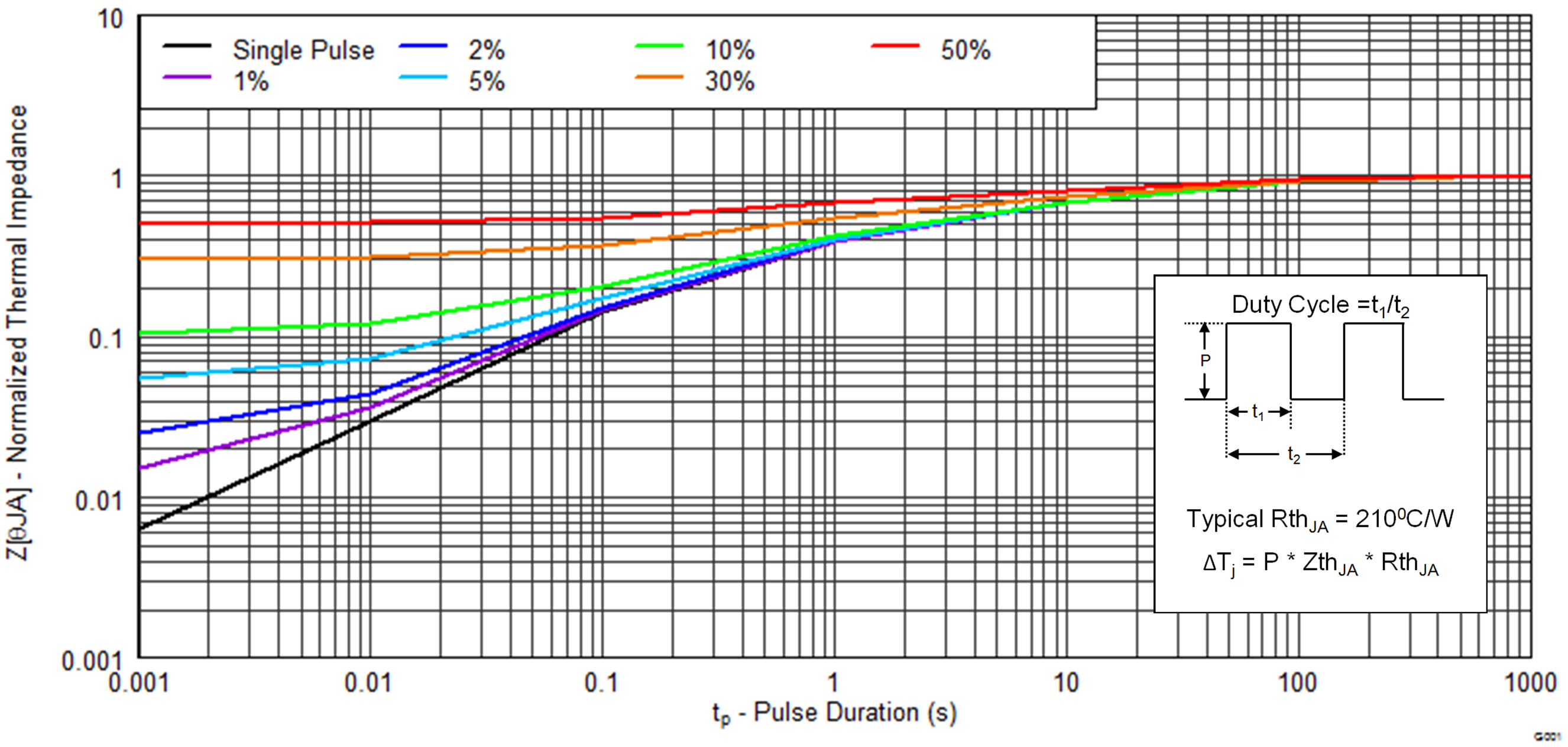

6 Device and Documentation Support
6.1 Trademarks
All other trademarks are the property of their respective owners.
6.2 Electrostatic Discharge Caution

These devices have limited built-in ESD protection. The leads should be shorted together or the device placed in conductive foam during storage or handling to prevent electrostatic damage to the MOS gates.
6.3 Glossary
SLYZ022 — TI Glossary.
This glossary lists and explains terms, acronyms, and definitions.