SLOS879B April   2014  – September 2016 DRV2625

PRODUCTION DATA.  

  1. Features
  2. Applications
  3. Description
  4. Revision History
  5. Pin Configuration and Functions
  6. Specifications
    1. 6.1 Absolute Maximum Ratings
    2. 6.2 ESD Ratings
    3. 6.3 Recommended Operating Conditions
    4. 6.4 Thermal Information
    5. 6.5 Electrical Characteristics
    6. 6.6 Timing Requirements
    7. 6.7 Switching Characteristics
    8. 6.8 Typical Characteristics
  7. Parameter Measurement Information
    1. 7.1 Test Setup for Graphs
      1. 7.1.1 Default Test Conditions
  8. Detailed Description
    1. 8.1 Overview
    2. 8.2 Functional Block Diagram
    3. 8.3 Feature Description
      1. 8.3.1  Support for ERM and LRA Actuators
      2. 8.3.2  Smart-Loop Architecture
        1. 8.3.2.1 Auto-Resonance Engine for LRA
        2. 8.3.2.2 Real-Time Resonance-Frequency Reporting for LRA
        3. 8.3.2.3 Automatic Switch to Open-Loop for LRA
        4. 8.3.2.4 Automatic Overdrive and Braking
          1. 8.3.2.4.1 Startup Boost
          2. 8.3.2.4.2 Brake Factor
        5. 8.3.2.5 Automatic Level Calibration
          1. 8.3.2.5.1 Automatic Compensation for Resistive Losses
          2. 8.3.2.5.2 Automatic Back-EMF Normalization
          3. 8.3.2.5.3 Calibration Time Adjustment
          4. 8.3.2.5.4 Loop-Gain Control
          5. 8.3.2.5.5 Back-EMF Gain Control
        6. 8.3.2.6 Actuator Diagnostics
        7. 8.3.2.7 Automatic Re-Synchronization
      3. 8.3.3  Open-Loop Operation
        1. 8.3.3.1 Waveform Shape Selection for LRA
        2. 8.3.3.2 Automatic Braking in Open Loop
      4. 8.3.4  Flexible Front-End Interface
        1. 8.3.4.1 Internal Memory Interface
          1. 8.3.4.1.1 Library Parameterization
          2. 8.3.4.1.2 Playback Interval
          3. 8.3.4.1.3 Waveform Sequencer
        2. 8.3.4.2 Real-Time Playback (RTP) Interface
        3. 8.3.4.3 Process Trigger
      5. 8.3.5  Noise Gate Control
      6. 8.3.6  Edge Rate Control
      7. 8.3.7  Constant Vibration Strength
      8. 8.3.8  Battery Voltage Reporting
      9. 8.3.9  Ultra Low-Power Shutdown
      10. 8.3.10 Automatic Go-To-Stand-by (Low Power)
      11. 8.3.11 I2C Watchdog Timer
      12. 8.3.12 Device Protection
        1. 8.3.12.1 Thermal Sensor
        2. 8.3.12.2 Over-Current Protection
        3. 8.3.12.3 VDD UVLO Protection
        4. 8.3.12.4 Brownout Protection
      13. 8.3.13 POR
      14. 8.3.14 Silicon Revision Control
      15. 8.3.15 Support for LRA and ERM Actuators
      16. 8.3.16 Multi-Purpose Pin Functionality
        1. 8.3.16.1 Trigger-Pulse Functionality
        2. 8.3.16.2 Trigger-Level (Enable) Functionality
        3. 8.3.16.3 Interrupt Functionality
      17. 8.3.17 Automatic Transition to Standby State
      18. 8.3.18 Automatic Brake into Standby
      19. 8.3.19 Battery Monitoring and Power Preservation
    4. 8.4 Device Functional Modes
      1. 8.4.1 Power States
      2. 8.4.2 Operation With VDD < 2.5 V (Minimum VDD)
      3. 8.4.3 Operation With VDD > 6 V (Absolute Maximum VDD)
      4. 8.4.4 Operation in Shutdown State
      5. 8.4.5 Operation in STANDBY State
      6. 8.4.6 Operation in ACTIVE State
      7. 8.4.7 Changing Modes of Operation
    5. 8.5 Operation During Exceptional Conditions
      1. 8.5.1 Operation With No Actuator Attached
      2. 8.5.2 Operation With a Non-Moving Actuator Attached
      3. 8.5.3 Operation With a Short at REG Pin
      4. 8.5.4 Operation With a Short at OUT+, OUT-, or Both
    6. 8.6 Programming
      1. 8.6.1 Auto-Resonance Engine Programming for the LRA
        1. 8.6.1.1 Drive-Time Programming
        2. 8.6.1.2 Current-Dissipation Time Programming
        3. 8.6.1.3 Blanking Time Programming
        4. 8.6.1.4 Zero-Crossing Detect-Time Programming
      2. 8.6.2 Automatic-Level Calibration Programming
        1. 8.6.2.1 Rated Voltage Programming
        2. 8.6.2.2 Overdrive Voltage-Clamp Programming
      3. 8.6.3 I2C Interface
        1. 8.6.3.1 TI Haptic Broadcast Mode
        2. 8.6.3.2 I2C Communication Availability
        3. 8.6.3.3 General I2C Operation
        4. 8.6.3.4 Single-Byte and Multiple-Byte Transfers
        5. 8.6.3.5 Single-Byte Write
        6. 8.6.3.6 Multiple-Byte Write and Incremental Multiple-Byte Write
        7. 8.6.3.7 Single-Byte Read
        8. 8.6.3.8 Multiple-Byte Read
      4. 8.6.4 Programming for Open-Loop Operation
        1. 8.6.4.1 Programming for ERM Open-Loop Operation
        2. 8.6.4.2 Programming for LRA Open-Loop Operation
      5. 8.6.5 Programming for Closed-Loop Operation
      6. 8.6.6 Diagnostics Routine
      7. 8.6.7 Calibration Routine
      8. 8.6.8 Waveform Playback Programming
        1. 8.6.8.1 Data Formats for Waveform Playback
        2. 8.6.8.2 Open-Loop Mode
        3. 8.6.8.3 Closed-Loop Mode
      9. 8.6.9 Waveform Setup and Playback
        1. 8.6.9.1 Waveform Playback Using RTP Mode
        2. 8.6.9.2 Waveform Sequencer
        3. 8.6.9.3 Waveform Playback Triggers
          1. 8.6.9.3.1 Playback Trigger Without Automatic Brake into Standby
            1. 8.6.9.3.1.1 Playback Trigger With Automatic Brake into Standby (SimpleDrive)
    7. 8.7 Register Map
      1. 8.7.1  Address: 0x00
      2. 8.7.2  Address: 0x01
      3. 8.7.3  Address: 0x02
      4. 8.7.4  Address: 0x03
      5. 8.7.5  Address: 0x04
      6. 8.7.6  Address: 0x05
      7. 8.7.7  Address: 0x06
      8. 8.7.8  Address: 0x07
      9. 8.7.9  Address: 0x08
      10. 8.7.10 Address: 0x09
      11. 8.7.11 Address: 0x0A
      12. 8.7.12 Address: 0x0B
      13. 8.7.13 Address: 0x0C
      14. 8.7.14 Address: 0x0D
      15. 8.7.15 Address: 0x0E
      16. 8.7.16 Address: 0x0F
      17. 8.7.17 Address: 0x10
      18. 8.7.18 Address: 0x11
      19. 8.7.19 Address: 0x12
      20. 8.7.20 Address: 0x13
      21. 8.7.21 Address: 0x14
      22. 8.7.22 Address: 0x15
      23. 8.7.23 Address: 0x16
      24. 8.7.24 Address: 0x17
      25. 8.7.25 Address: 0x18
      26. 8.7.26 Address: 0x19
      27. 8.7.27 Address: 0x1A
      28. 8.7.28 Address: 0x1B
      29. 8.7.29 Address: 0x1C
      30. 8.7.30 Address: 0x1D
      31. 8.7.31 Address: 0x1F
      32. 8.7.32 Address: 0x20
      33. 8.7.33 Address: 0x21
      34. 8.7.34 Address: 0x22
      35. 8.7.35 Address: 0x23
      36. 8.7.36 Address: 0x24
      37. 8.7.37 Address: 0x25
      38. 8.7.38 Address: 0x26
      39. 8.7.39 Address: 0x27
      40. 8.7.40 Address: 0x28
      41. 8.7.41 Address: 0x29
      42. 8.7.42 Address: 0x2A
      43. 8.7.43 Address: 0x2C
      44. 8.7.44 Address: 0x2E
      45. 8.7.45 Address: 0x2F
      46. 8.7.46 Address: 0x30
  9. Application and Implementation
    1. 9.1 Application Information
    2. 9.2 Typical Application
      1. 9.2.1 Design Requirements
      2. 9.2.2 Detailed Design Procedure
        1. 9.2.2.1 Actuator Selection
          1. 9.2.2.1.1 Eccentric Rotating-Mass Motors (ERM)
          2. 9.2.2.1.2 Linear Resonance Actuators (LRA)
            1. 9.2.2.1.2.1 Auto-Resonance Engine for LRA
        2. 9.2.2.2 Capacitor Selection
        3. 9.2.2.3 Interface Selection
        4. 9.2.2.4 Power Supply Selection
      3. 9.2.3 Application Curves
    3. 9.3 Initialization Set Up
      1. 9.3.1 Initialization Procedure
      2. 9.3.2 Typical Usage Examples
        1. 9.3.2.1 Play a Waveform or Waveform Sequence from the ROM Waveform Memory
        2. 9.3.2.2 Play a Real-Time Playback (RTP) Waveform
  10. 10Power Supply Recommendations
  11. 11Layout
    1. 11.1 Layout Guidelines
    2. 11.2 Layout Examples
  12. 12Device and Documentation Support
    1. 12.1 Device Support
      1. 12.1.1 Waveform Library Effects List
    2. 12.2 Trademarks
    3. 12.3 Electrostatic Discharge Caution
    4. 12.4 Glossary
  13. 13Mechanical, Packaging, and Orderable Information

パッケージ・オプション

デバイスごとのパッケージ図は、PDF版データシートをご参照ください。

メカニカル・データ(パッケージ|ピン)
  • YFF|9
サーマルパッド・メカニカル・データ
発注情報

1 Features

  • Ultra Low-Power Shutdown Mode
  • Low-Power Standby State
  • Resistance-Based Actuator Diagnostics
  • SimpleDrive One-Wire Vibration Scheme
  • Automatic Resonance Tracking and Reporting
  • Automatic Overdrive and Braking
  • Automatic Level Calibration
  • Drive Compensation Over Battery Discharge
  • Configurable Battery Monitor with Power Preservation
  • Off-Resonance Driving with Auto-Braking
  • LRA Waveform Shape Selection
  • Licensed Immersion TouchSense® 2200
  • Built-In Library with Loopable Waveform Sequencer
  • Real-Time Playback (RTP) Mode
  • I2C-Controlled Digital Playback Engine
  • Hardware and Software Trigger Option
  • Automatic Transition to Standby with Auto-Brake
  • Optional Interrupt Pin
  • 1.8-V Compatible, VDD Tolerant Digital Interface (1)
(1)
(1) Patent pending control algorithm

2 Applications

  • Mobile Phones and Tablets
  • Fitness Bands and Wearable Devices
  • Remote Controls, Mice, and Peripheral Devices
  • Touch-Enabled Devices
  • Human-Machine Interfaces

3 Description

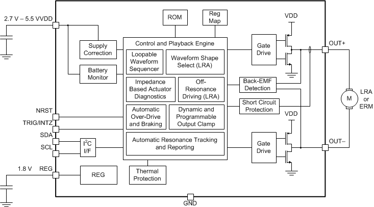
The DRV2625 device is a haptic driver that relies on a proprietary closed-loop architecture to deliver sharp, strong, and consistent haptic effects while optimizing power consumption.

The internal library and loopable waveform sequencer, together with the automatic overdrive and braking simplifies the process of generating crisp and optimum haptic effects, reducing the burden imposed into the processing unit.

The DRV2625 device features an automatic go-to-standby state and a battery preservation function to help reduce power consumption without user intervention. The NRST pin allows for a full shutdown state for additional power savings.

The waveform shape selection allows for sine-wave and square-wave drive to customize the haptic feel as well as the audible performance. Off-resonance driving with automatic braking simplifies the implementation of non-resonant haptic solutions.

Device Information(1)

DEVICE NAME PACKAGE BODY SIZE (MAX)
DRV2625 DSBGA (9) 1.498 mm × 1.361 mm
(1) For all available packages, see the orderable addendum at the end of the datasheet.

Simplified Schematic

DRV2625 Simplified_Schematic_slos893.gif