SLOS690C December 2010 – July 2016 DRV612
UNLESS OTHERWISE NOTED, this document contains PRODUCTION DATA.
- 1 Features
- 2 Applications
- 3 Description
- 4 Revision History
- 5 Device Comparison Table
- 6 Pin Configuration and Functions
- 7 Specifications
- 8 Parameter Measurement Information
- 9 Detailed Description
- 10Application and Implementation
- 11Power Supply Recommendations
- 12Layout
- 13Device and Documentation Support
- 14Mechanical, Packaging, and Orderable Information
パッケージ・オプション
メカニカル・データ(パッケージ|ピン)
サーマルパッド・メカニカル・データ
- RGT|16
発注情報
1 Features
- DirectPath™
- Eliminates Pops and Clicks
- Eliminates Output DC-Blocking Capacitors
- 3-V to 3.6-V Supply Voltage
- Low Noise and THD
- SNR > 105 dB at –1× Gain
- Vn < 12 μVms, 20 Hz to 20 kHz at –1× Gain (Typical)
- THD+N < 0.003% at 10-kΩ Load and –1× Gain
- 2-Vrms Output Voltage Into 600-Ω Load
- Single-Ended Input and Output
- Programmable Gain Select Reduces Component Count
- 13× Gain Values
- Active Mute With More Than 80-dB Attenuation
- Short-Circuit and Thermal Protection
- ±8-kV HBM ESD-Protected Outputs
2 Applications
- PDP and LCD TVs
- DVD Players
- Mini and Micro Combo Systems
- Soundcards
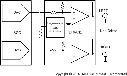
Functional Block Diagram

3 Description
The DRV612 is a single-ended, 2-Vrms stereo line driver designed to reduce component count, board space, and cost. It is ideal for single-supply electronics where size and cost are critical design parameters.
The DRV612 does not require a power supply greater than 3.3 V to generate its 5.6-VPP output, nor does it require a split-rail power supply.
The DRV612 device is designed using TI’s patented DirectPath technology, which integrates a charge pump to generate a negative supply rail that provides a clean, pop-free ground-biased output. The DRV612 is capable of driving 2 Vms into a 600-Ω load. DirectPath technology also allows the removal of the costly output dc-blocking capacitors.
The device has fixed-gain single-ended inputs with a gain-select pin. Using a single resistor on this pin, the designer can choose from 13 internal programmable gain settings to match the line driver with the codec output level. The device also reduces the component count and board space.
Line outputs have ±8-kV HBM ESD protection, enabling a simple ESD protection circuit. The DRV612 has built-in active mute control with more that 80-dB attenuation for pop-free mute on/off control.
The DRV612 is available in a 14-pin TSSOP and 16-pin VQFN. For a footprint-compatible stereo headphone driver, see the TPA6139A2.
Device Information(1)
| PART NUMBER | PACKAGE | BODY SIZE (NOM) |
|---|---|---|
| DRV612 | TSSOP (14) | 5.00 mm × 4.40 mm |
| VQFN (16) | 3.00 mm × 3.00 mm |
- For all available packages, see the orderable addendum at the end of the data sheet.
4 Revision History
Changes from B Revision (April 2011) to C Revision
- Added ESD Ratings table, Feature Description section, Device Functional Modes, Application and Implementation section, Power Supply Recommendations section, Layout section, Device and Documentation Support section, and Mechanical, Packaging, and Orderable Information section.Go
- Removed Ordering Information table, see POA at the end of the data sheet Go
Changes from A Revision (February 2011) to B Revision
- Changed RIN = 10 kΩ, Rfb = 20 kΩ To Gain = -2V/V in the Typical Characteristics condition textGo
Changes from * Revision (December 2010) to A Revision
- Added the QFN pinout drawingGo
- Added the QFN device to the Pin Functions tableGo
- Changed minimum storage temperature from –40°C to –65°CGo
- Changed the Gain resistor 2% tolerance values in the Programmable Gain Settings table for Gain Steps and Input ImpedanceGo
- Changed Note 1 of the PROGRAMMABLE GAIN SETTINGS table From: If pin 12, GAIN, is left floating To: If the GAIN pin is left floatingGo
- Changed From: CPUMP = C(VSS) = 10 µF To: CPUMP = C(VSS) = 1 µF in the Typical Characteristics condition textGo
- Changed the Gain_set RESISTOR values in Table 2Go
- Changed the Gain_set RESISTOR values in Table 3Go
- Removed references to DRV614 from the FOOTPRINT COMPATIBLE WITH TPA6139A2 sectionGo