SLOS842A September 2013 – June 2015 DRV8301-Q1
PRODUCTION DATA.
- 1 Features
- 2 Applications
- 3 Description
- 4 Revision History
- 5 Pin Configuration and Functions
-
6 Specifications
- 6.1 Absolute Maximum Ratings
- 6.2 ESD Ratings
- 6.3 Recommended Operating Conditions
- 6.4 Thermal Information
- 6.5 Electrical Characteristics
- 6.6 Buck Converter Characteristics
- 6.7 Current Shunt Amplifier Characteristics
- 6.8 Gate Timing and Protection Characteristics
- 6.9 SPI Timing Requirements (Slave Mode Only)
- 6.10 Typical Characteristics
- 7 Detailed Description
- 8 Application and Implementation
- 9 Power Supply Recommendations
- 10Layout
- 11Device and Documentation Support
- 12Mechanical, Packaging, and Orderable Information
パッケージ・オプション
メカニカル・データ(パッケージ|ピン)
- DCA|56
サーマルパッド・メカニカル・データ
- DCA|56
発注情報
1 Features
- Qualified for Automotive Applications
- AEC-Q100 Tested With the Following Results:
- Device Temperature Grade 1: –40°C to 125°C Ambient Operating Temperature Range
- Device HBM ESD Classification Level 2
- Device CDM ESD Classification Level C4A
- Operating Supply Voltage 6 to 60 V
- 2.3-A Sink and 1.7-A Source Gate Drive Current Capability
- Integrated Dual Shunt Current Amplifiers With Adjustable Gain and Offset
- Integrated Buck Converter to Support up to 1.5-A External Load
- Independent Control of 3 or 6 PWM Inputs
- Bootstrap Gate Driver With 100% Duty Cycle Support
- Programmable Dead Time to Protect External FETs from Shoot-Through
- Slew Rate Control for EMI Reduction
- Programmable Overcurrent Protection of External MOSFETs
- Support Both 3.3-V and 5-V Digital Interface
- SPI Interface
- Thermally Enhanced 56-Pin HTSSOP Pad-Down DCA Package
2 Applications
- Automotive 3-Phase Brushless DC Motor and Permanent Magnet Synchronous Motor
- Water, Oil, Fuel Pumps
3 Description
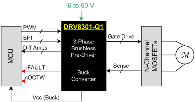
The DRV8301-Q1 device is an automotive gate driver IC for three phase motor drive applications. The device provides three half bridge drivers, each capable of driving two N-type MOSFETs, one for the high-side and one for the low side. The device supports up to 2.3-A sink and 1.7-A source peak current capability and only needs a single power supply with a wide range from 6 to 60 V. The DRV8301-Q1 device uses bootstrap gate drivers with trickle charge circuitry to support 100% duty cycle. The gate driver uses automatic hand shaking when high-side FET or low-side FET is switching to prevent current shoot through. VDS of FETs is sensed to protect external power stage during overcurrent conditions.
The DRV8301-Q1 device includes two current shunt amplifiers for accurate current measurement. The current amplifiers support bi-directional current sensing and provide an adjustable output offset of up to 3 V.
The DRV8301-Q1 device also has an integrated switching mode buck converter with adjustable output and switching frequency to support MCU or additional system power needs. The buck is capable to drive up to 1.5-A load.
The SPI interface provides detailed fault reporting and flexible parameter settings such as gain options for current shunt amplifier, slew rate control of gate driver, and other settings.
Device Information(1)
| PART NUMBER | PACKAGE | BODY SIZE (NOM) |
|---|---|---|
| DRV8301-Q1 | HTSSOP (56) | 14.00 mm × 6.10 mm |
- For all available packages, see the orderable addendum at the end of the data sheet.
Simplified Schematic
